|
| |
nextnano3 - Tutorial
next generation 3D nano device simulator
1D Tutorial
Energy dispersion of holes in a quantum well
Authors:
Stefan Birner,
Michael Povolotskyi
If you want to obtain the input files that are used within this tutorial, please
check if you can find them in the installation directory.
If you cannot find them, please submit a
Support Ticket.
-> a) 1Dwell_GaAs_AlAs_nn3.in  / *_nnp.in
-
input file for the nextnano3 and nextnano++ software
-> b) 1Dwell_GaSb_AlSb_nn3.in / *_nnp.in -
-> c) 1Dwell_InGaAs_InP_nn3.in / *_nnp.in -
-> d) 1DIn20Ga80AsQW_75nm_sg.in


   1DIn20Ga80AsQW_75nm_kp.in

      1DIn20Ga80AsQW_75nm_kp_dispersion.in
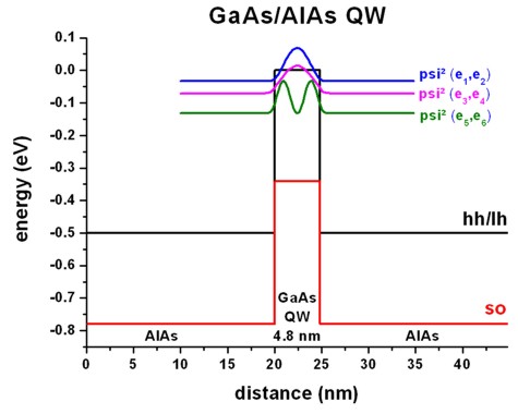
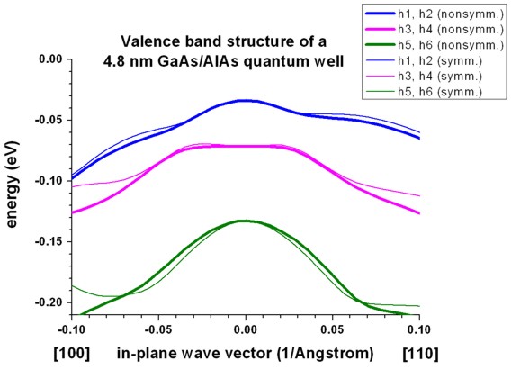
a) Unstrained GaAs/AlAs quantum well
b) Tensilely strained GaSb/AlSb quantum well
c) Tensilely strained In0.43Ga0.57As/InP quantum well
c) Strained In0.2Ga0.8As/GaAs quantum well
a) Unstrained GaAs/AlAs quantum well
b) Tensilely strained GaSb/AlSb quantum well
=> 1Dwell_GaSb_AlSb_nn3.in
The following figure reproduces Fig. 2 of Franceschi's paper very well.
It is a tensiley strained 5.1 nm GaSb quantum well embedded between
unstrained AlSb barriers.
The biaxial strain is 0.65 % and breaks the degeneracy of the bulk heavy and
light hole band edge. Now the light hole band edge lies above the heavy hole
band edge.
The figure shows that the first two subbands are nearly degenerate at the
Brillouin zone center and show strong coupling.
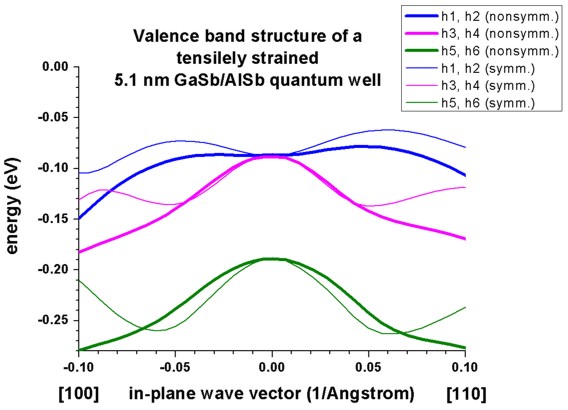
A large discrepancy between the nonsymmetrized and the symmetrized
k.p Hamiltonian can be seen. (See also the discussion in Franceschi's paper
and their tight-binding results.)
c) Tensilely strained In0.43Ga0.57As/InP quantum well
=> 1Dwell_InGaAs_InP_nn3.in
The following figure reproduces Fig. 3 of Franceschi's paper very well.
It is a tensiley strained 5.7 nm In0.43Ga0.57As quantum
well embedded between unstrained InP barriers.
The biaxial strain is 0.73 % and breaks the degeneracy of the bulk heavy and
light hole band edge. Now the light hole band edge lies above the heavy hole
band edge.
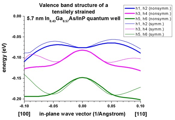
Again, a large discrepancy between the nonsymmetrized and the
symmetrized k.p Hamiltonian can be seen. (See also the discussion in
Franceschi's paper and their tight-binding results.)
d) Strained In0.2Ga0.8As/GaAs quantum well
=> 1DIn20Ga80AsQW_75nm_sg.in

   1DIn20Ga80AsQW_75nm_kp.in

   1DIn20Ga80AsQW_75nm_kp_dispersion.in
These input files have been used for Fig. 8 in the following paper:
Dimensionally constrained D’yakonov–Perel’ spin relaxation in n-InGaAs
channels: transition from 2D to 1D
A.W. Holleitner, V. Sih, R.C. Myers, A.C. Gossard, D.D. Awschalom
New Journal of Physics 9, 342 (2007)
=> 1DIn20Ga80AsQW_75nm_sg.in
A 7.5 nm In0.2Ga0.8As quantum well is sandwiched
between two GaAs layers. The quantum well is grown pseudomorphically on a GaAs
substrate and is thus strained compressively with respect to the GaAs
substrate.
The GaAs is n-type doped with Si with a concentration of 3 x 10¹⁷
cm-3 in the regions between 50 and 80 nm and between 127.5 and
137.5 nm.
Consequently, we first have to solve the single-band Schrödinger equation
together with the Poisson equation self-consistently, in order to obtain the
electrostatic potential. The electron ground state is below the Fermi level.
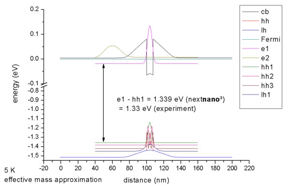
=> 1DIn20Ga80AsQW_75nm_kp.in
The calculated electrostatic potential is read in and then the 8-band k.p
equation is solved to get the eigenstates for k||=0.
The calculated transition energy between the ground state electron and the
ground state (heavy) hole is 1.340 eV. (Note: The exciton correction has not
been considered and is of the order 4 meV.)
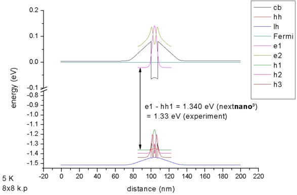
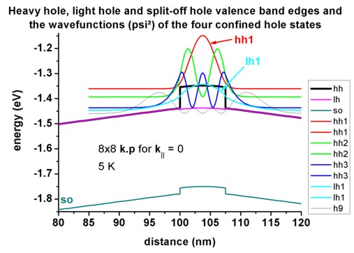
For k||=0, the three highest hole states have heavy hole
character whereas the forth state has light hole character. No further states
are confined. The split-off hole band edge is far away from the heavy and
light hole band edges (~ 0.3 eV).
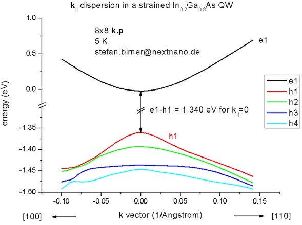
=> 1DIn20Ga80AsQW_75nm_kp_dispersion.in
We read in the electrostatic potential again and calculate the 8-band k.p
dispersion for k||/=0. This time the calculation is more
time-consuming as the Schrödinger equation has to be solved for 250 different
k|| points, i.e. the CPU time is 250 times larger than for
k||=0 only.
For | k|| | <= 0.02 1/Angstrom, the directions
[10] and [11] are practically identical for the uppermost hole level.
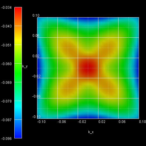
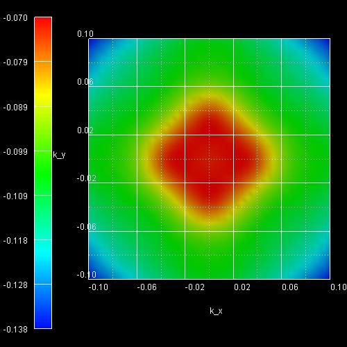
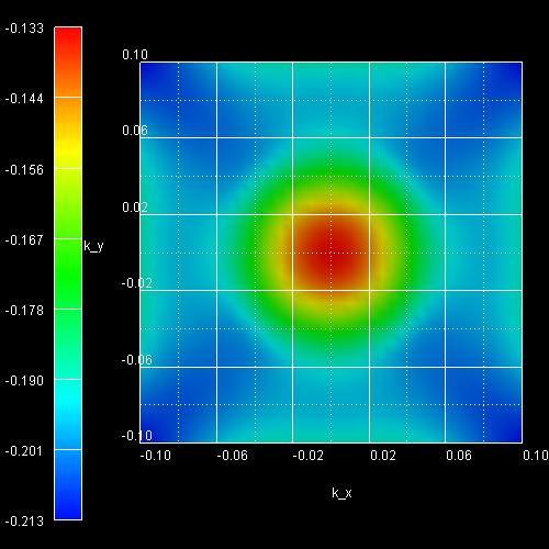
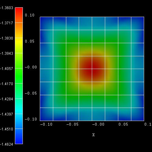
- The following figure shows the k|| dispersion of the
highest hole state (h1).
The x axis shows the kx value between -0.10
[1/Angstrom] and 0.10 [1/Angstrom], the y axis shows ky.
The maximum energy of the hole state occurs at -1.3603
eV at (kx,ky) = (0,0), i.e. in the center of the
figure (Gamma point).
|