nextnano3 - Tutorial
2D Tutorial
Electron wave functions of a 2D slice of a Triple Gate MOSFET
Author:
Stefan Birner
==> This is the old website:
A new version of this tutorial can be found
here.
 -> 2DSi_TGMOS_2Dcut_atGate_cl.in

 -> 2DSi_TGMOS_2Dcut_atGate_qm.in

 -> 2DSi_TGMOS_2Dcut_atGate_qm_iso.in

 -> 3DSi_TGMOS_5nm_SD0V_G0V_qm.in

 -> 3DSi_TGMOS_5nm_SD0V_G05V_qm.in
Triple Gate MOSFET (2D simulation)
A Triple Gate MOSFET is a nanowire if the dimensions along the x and y
directions are only a few nanometers, thus quantization effects have to be taken
into account.
The Si channel has a rectangular shape
with a width of 5 nm and a height of 5 nm.
The Si channel is surrounded by SiO2
(thickness 1.5 nm).
The Si/SiO2 nanowire is surrounded by a Gate
(at the left and right side, and at the top).
The following schematic shows a 2D slice of a 3D Triple Gate MOSFET.
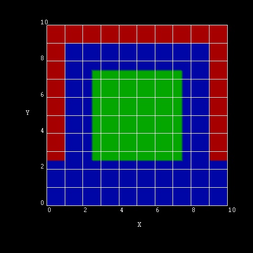
In this tutorial we will only simulate this 2D slice and not the whole 3D
structure.
We apply a voltage of 0.5 V to the Gates and solve the two-dimensional Schrödinger and
Poisson equations self-consistently (including the SiO2 region).
There are six conduction band minima in silicon (Delta valleys).
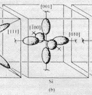
Consequently, we have to solve three 2D Schrödinger equations with
different effective mass tensor orientations because the mass tensor is not
isotropic.
The longitudial mass is 0.916 m0.
The transversal mass is 0.190 m0
Our Schrödinger equations are numbered deg1, deg2,
deg3.
deg1: a) mxx = mlongitudinal = 0.916 m0, myy = mtransversal
= 0.190 m0
deg2: b) mxx = mtransversal = 0.190 m0, myy = mlongitudinal
= 0.916 m0
deg3: c) mxx = myy = mtransversal
= 0.190 m0
The potential Ec(x,y) that enters the Schrödinger equation is
the same in these three cases.
Note: The cases a) and b) are not identical (i.e. degenerate) because the
potential is not symmetric with respect to exchanging x and y coordinates.
The following keyword and specifier can be used to output the effective mass
tensors (1/mij). This is important to check how the Schrödinger
equations are sorted with respect to their effective masses.
$output-1-band-schroedinger

   ...

   effective-mass-tensor = yes
Electron wave functions (psi²)
-> 2DSi_TGMOS_2Dcut_atGate_qm.in
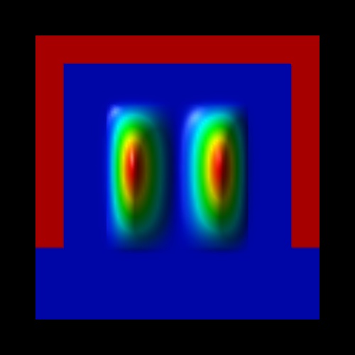
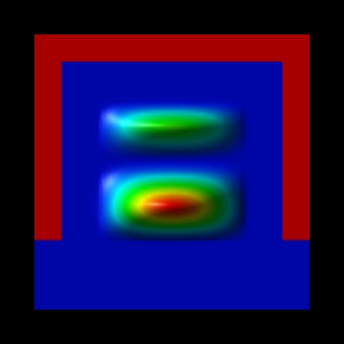
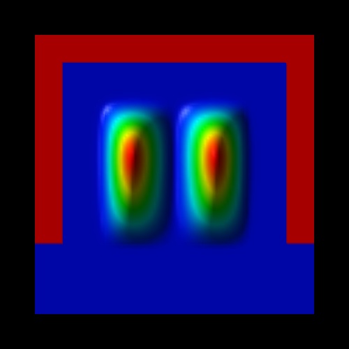
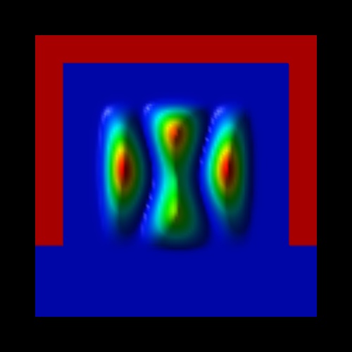
The lowest eigenstates for the cases a), b) and c) are the following:
deg1: a) mxx = mlongitudinal = 0.916 m0, myy = mtransversal
= 0.190 m0
Here, the heavier mass is along the y directon, and the lighter mass along the y
direction.
The energy spacing between the two lowest subbands is about 25 meV.
The eigenvalues are contained in Schroedinger_1band/ev2D_cb003_qc001_sg001_deg001_dir_Kx001_Ky001_Kz001.dat.
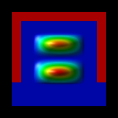
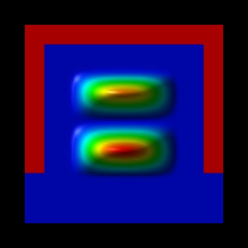
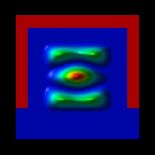
deg2: b) mxx = mtransversal = 0.190 m0, myy = mlongitudinal
= 0.916 m0
Here, the lighter mass is along the x directon, and the heavier mass along the y
direction.
The energy spacing between the two lowest subbands is about 35 meV.
The eigenvalues are contained in Schroedinger_1band/ev2D_cb003_qc001_sg001_deg002_dir_Kx001_Ky001_Kz001.dat.
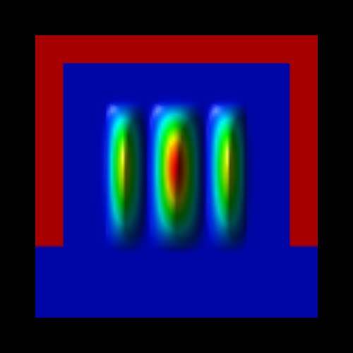
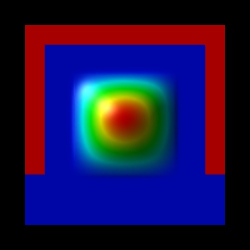
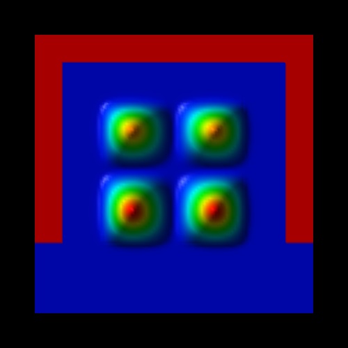
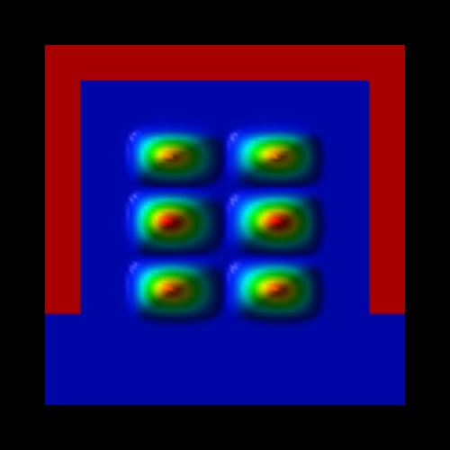
deg3: c) mxx = myy = mtransversal
= 0.190 m0
E4,deg3 = 323, E5,deg3
= 462, E6,deg3
= 470, E7,deg3
= 615, E8,deg3
= 616
These eigenvalues have the lighter mass in the x and y directions.
Consequently, their energies are much higher than in the other two Schrödinger
equations.
The energy spacings between the lowest subbands is of the order 140-150 meV.
The eigenvalues are contained in Schroedinger_1band/ev2D_cb003_qc001_sg001_deg003_dir_Kx001_Ky001_Kz001.dat.
(Compare the wave functions and the energies with the isotropic case as discussed
further below.)
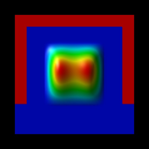
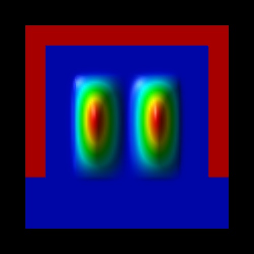
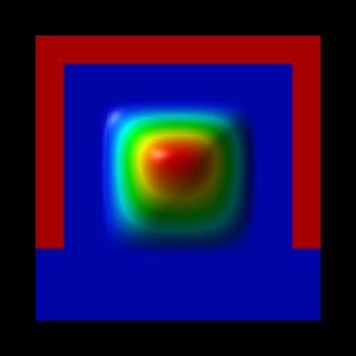
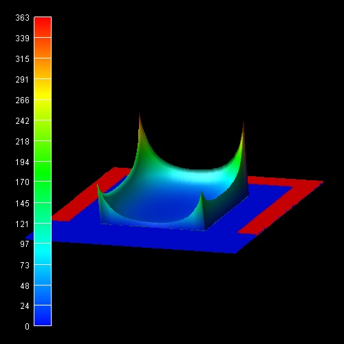
Electron density
The resulting electron density has the following shape:
The units are 1 x 1018 cm-3. The density has been
calculated by occupying the eigenstates with respect to the Fermi level which is
at 0 eV.
Note that the quantum mechanical density is close to zero near the Si/SiO2
interfaces because the wave functions tend to zero at the SiO2
barriers.
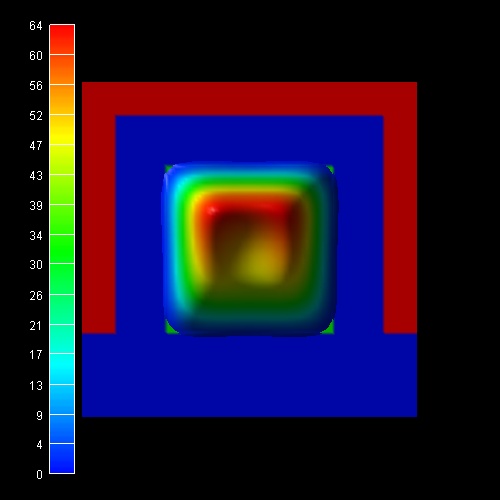
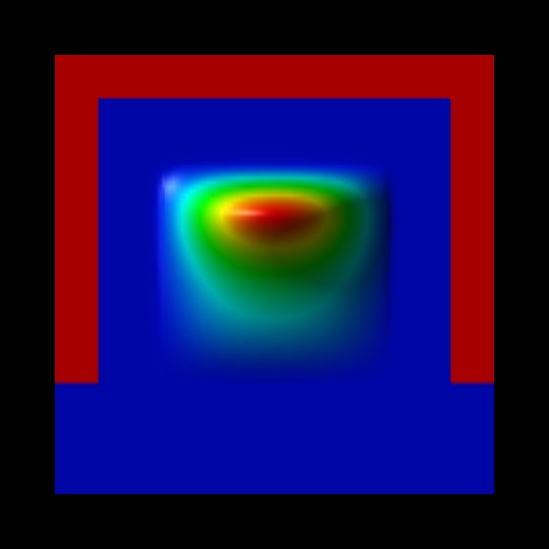
The following figure shows the same quantum mechanical electron density
together with two slices through the conduction band edges.
The units are in eV and the conduction band offset between SiO2 and
Si is 3.1 eV.
At the gates, the conduction band edge is set to -0.5 eV, representing the
applied bias of 0.5 eV.
One can clearly see that for silicon in the middle of the nanowire the
conduction band has its highest value and its lowest value close at the Si/SiO2
interface.
If one had neglected the effect of quantum confinement, then the resulting
classical electron density would have peaks near the Si/SiO2
interfaces as is shown in this figure.
-> 2DSi_TGMOS_2Dcut_atGate_cl.in
Obviously, a realistic calculation of such transistors cannot be based on
classical densities. The full 2D (or better 3D) Schrödinger equations have to be
solved. The IV characteristics of such a quantum-mechanically calculated Triple Gate MOSFET transistor will be discussed in another tutorial.
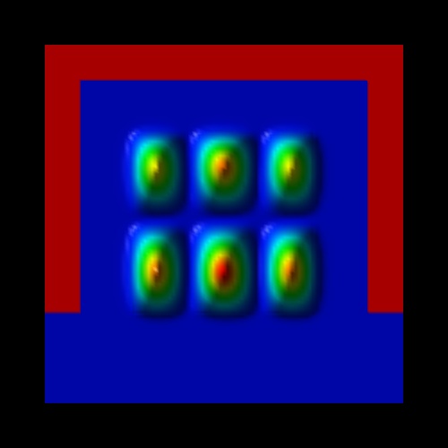
Isotropic electron masses
-> 2DSi_TGMOS_2Dcut_atGate_qm_iso.in
Very often, for simplicity, an isotropic electron mass for the Schrödinger
equation is assumed.
E.g. the DOS (density of states) electron mass of Si in the Delta minima can be
calculated as follows:
me*DOS
= (ml·mt2)1/3 = (0.916·0.192)1/3
m0 = 0.321m0
More details...
In this case, only one Schrödinger equation has to be solved (in contrast
to three equations as described above), thus deg = 1.
The wave functions and energies in this case are:
deg1: mxx = myy = mDOS
= 0.321 m0
The wave functions (psi²) look very similar as in the case of "deg3:
c)" (see above) where the masses are isotropic in the (x,y)
plane but here, the energy spacings between different subbands are smaller
(around 90-100 meV) because the DOS mass is larger than the transversal masses
(as in the case of "deg3: c)").
The eigenvalues are contained in Schroedinger_1band/ev2D_cb003_qc001_sg001_deg001_dir_Kx001_Ky001_Kz001.dat.
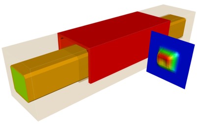
3D simulation of the Triple Gate MOSFET
 -> 3DSi_TGMOS_5nm_SD0V_G0V_qm.in

 -> 3DSi_TGMOS_5nm_SD0V_G05V_qm.in
The following figures show the results of the self-consistent 3D
Schrödinger-Poisson solution of this Triple Gate structure
(Si channel length = 25 nm, source region length = 10 nm, drain region length =
10 nm,
constant doping profile in source and drain region with a doping
concentration of 1 * 1020 cm-3 (fully ionized)
| |
Note: Compare this electron density with the density obtained in the 2D
simulation as discussed above. |
 |
 |
|
closed channel
VSD = 0.0 V
VSG = 0.0 V
|
open channel
VSD = 0.0 V
VSG = 0.5 V
|
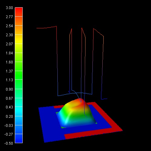
The plots show the isosurfaces of the electron densities along 2D slices through
the Triple Gate MOSFET. The lower two figures also show 1D slices of the
conduction band profiles and 1D slices of the electron densities in the middle
of the device.
The classical densities would look similar to the classical densities of the 2D
calculations shown above.
|