nextnano3 - Tutorial
next generation 3D nano device simulator
1D Tutorial
Scattering times for electrons in unbiased and biased single and multiple
quantum wells
Author:
Stefan Birner
If you want to obtain the input files that are used within this tutorial, please
check if you can find them in the installation directory.
If you cannot find them, please submit a
Support Ticket.
-> 1DGaAs_AlGaAs_10nmQW_Lifetime.in

-> 1DGaAs_AlGaAs_12nmQW_LifetimeFig5_field.in

-> 1DGaAs_AlGaAs_SingleQW_7nm.in

-> 1DGaAs_AlGaAs_DoubleQW_7nm_nonsymmetric.in

-> 1DGaAs_AlGaAs_DoubleQW_LifetimeFig12_field.in
Scattering times for electrons in unbiased and biased single and multiple
quantum wells
This tutorial tries to reproduce the results of
[FerreiraBastard1989]
R. Ferreira, G. Bastard
Evaluation of some scattering times for electrons in unbiased and biased
single- and multiple-quantum-well structures
Physical Review B 40 (2), 1074 (1989)
Scattering time as a function of quantum well width
-> 1DGaAs_AlGaAs_10nmQW_Lifetime.in
First, we want to study the electron lifetimes (scattering rates) of a single
quantum well as a function of quantum well width
%QW_width.
(Note: Use nextnanomat's Template feature to automatically sweep over the
quantum well width.)
Our quantum well consists of GaAs that is sandwiched between two Al0.3Ga0.7As
barriers.
The material parameters that we are using for this tutorial are identical to the
ones used in the above cited paper:
- electron mass:
me = 0.07 m0
- conduction band offset: CBO
= 0.2138 eV
- static dielectric constant: epsilon = 12.5
- LO phonon energy:
hbarw0 = 0.036 eV
(longitudinal optical phonon)
For the calculations, a grid resolution of 0.1 nm has been used.
$output-1-band-schroedinger

 ...

 intraband-matrix-elements = yes  !
calculates the intersubband transition matrix elements
 intraband-lifetime
= yes  !
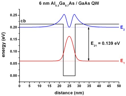
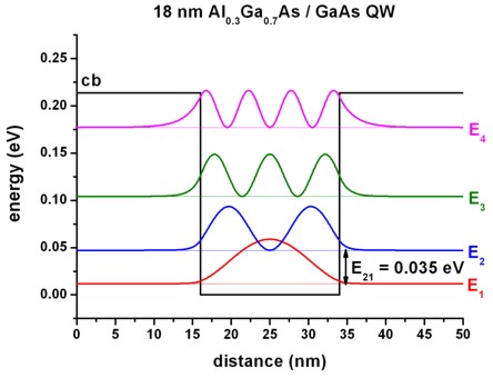
The following two figures show the conduction band edges and the lowest
confined eigenstates (including the square of the wave functions) for a 6 nm and
an 18 nm AlGaAs/GaAs quantum well.
The quantum well width can be varied easily by making use of the variable
 %QW_width = 10 !
(DisplayUnit:nm) (ListOfValues:5.2,5.4,5.6,5.8,6,7,8,10,12,14,15,16,17,18,19,20)
Note that we make use of the specifier
region-priority:
==> Higher priority overwrites lower priority regions.
   $regions


    region-number = 1
base-geometry = line
region-priority = 1  !

    z-coordinates = 0d0 50d0
! from  0 to 50 nm
! 50 nm AlGaAs
    region-number = 2
base-geometry = line
region-priority = 2  !
higher
priority
  ! z-coordinates = 22d0 28d0
   ! from 22 to 28 nm
!  6 nm GaAs

    z-coordinates = 20d0 30d0
! from 20 to 30 nm
! 10 nm GaAs

  ! z-coordinates = 16d0 34d0
! from 16 to 34 nm
! 18 nm GaAs
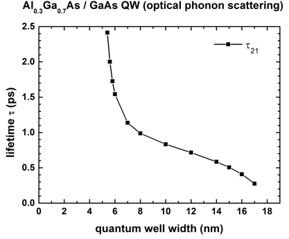
The following figure shows the electron lifetime of the second eigenstate (E2
= initial state) to the ground state (E1 = final state), i.e. the
intersubband transition 2 ->
1 (with energy E21) for
different quantum well widths. The temperature is set to 0 K.
For quantum well widths smaller than 5.4 nm (Ferreira: 5.5 nm), only the ground
state is confined and E2 is unbound.
For quantum well widths larger than 18 nm (Ferreira: 17.8 nm), the transition
energy E21 is smaller than the LO phonon energy of 36 meV, thus
scattering through the emission of an LO phonon is not possible any more.
The nextnano³ calculations are in good agreement with Fig. 3 of the paper
by R. Ferreira and G. Bastard.
The output of the electron lifetime can be found in this file:
Schroedinger_1band/intraband_pz1D_cb001_qc001_sg001_deg001_dir.txt


	...


	Intersubband dipole moment  | < psi_f* | pz | psi_i > |  [h_bar /
	nm]

	------------------|----------------------------------------------------------------------


	Oscillator strength []

	------------------|--------------|-------------------------------------------------------


	Energy of transition [eV]

	------------------|--------------|-------------|-----------------------------------------


	m* [m_0]      lifetime [ps]

	------------------|--------------|-------------|-------------|-------------|-------------

	...

	<psi001*|pz|psi002> 0.19717291    0.985747159
	0.085864536   0.070000000   0.833765805

	...
Here, the shown values for the intersubband transitions correspond to a
10 nm QW.
Scattering times as a function of electric field magnitude
-> 1DGaAs_AlGaAs_12nmQW_LifetimeFig5_field.in
This input file will perform a sweep over the electric field strength.
The output for each sweep is labeled with ind00i, where i
indicates the number of the sweep.
This figure shows the lowest eigenstates of a 12 nm AlGaAs/GaAs QW at an
applied electric field of -50 kV/cm (ind005).
This time the conduction band edge is not flat any more. It is tilted because of
the electric field.
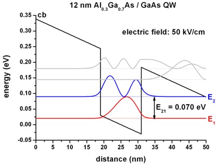
The following figure shows the scattering time of a 12 nm Al0.3Ga0.7As/GaAs
QW as a function of applied electric field.
The nextnano³ calculations are in reasonable agreement with Fig. 5 of
the paper by R. Ferreira and G. Bastard.
The sweep over the electric field magnitude can be done automatically. For
details, see
$electric-field.
For these calculations, a grid resolution of 0.10 nm had been used.
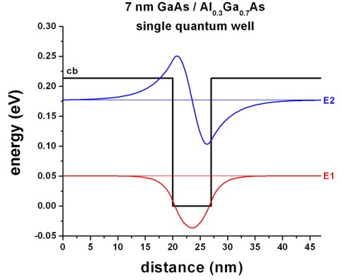
Single quantum wells
-> 1DGaAs_AlGaAs_SingleQW_7nm.in
Here, the two confined energy levels and wave functions of the 7 nm single
quantum well are shown.
The energy of the ground state is 50.4 meV.
Double quantum wells
-> 1DGaAs_AlGaAs_DoubleQW_7nm_nonsymmetric.in
Here, we study the electron energy levels of a nonsymmetric double quantum
well structure as a function of quantum well width of the
right quantum well %right_QW_width.
The right quantum well width can be varied easily by making use of the variable
 %right_QW_width = 7
! (DisplayUnit:nm) (ListOfValues:7.0,8.0,10.0,12.5,15.0,17.5,20.0,22.5,25.0,27.5,30.0,35.0,37.5,40.0,45.0,47.5,50.0,55.0,57.5,60.0,65.0,67.5,70.0,75.0,77.5,80.0,85.0,87.5,90.0,95.0,97.5,100.0)
For the following figures, a grid resolution of 0.25 nm had been used.
The following figure shows the energy levels of a nonsymmetric double quantum
well structure (GaAs / Al0.3Ga0.7As) where the left
quantum well always has the width 7 nm, and the right quantum well varies from 7
nm to 100 nm.
The two GaAs wells are separated by a 5 nm Al0.3Ga0.7As
barrier.
The figure shows the energy levels as a function of the width of the larger
quantum well.
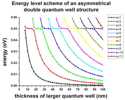
One can see, that for certain widths of the larger quantum well, an anticrossing
due to bonding and antibonding states occurs. This happens whenever an
eigenstate of the larger well matches the energy of the ground state of the
smaller (7 nm) quantum well (which is at 50.4 meV, see example shown above:
==> 1DGaAs_AlGaAs_SingleQW_7nm.in).
Our calculations are in very good agreement with Fig. 9 of Ferreira et al.
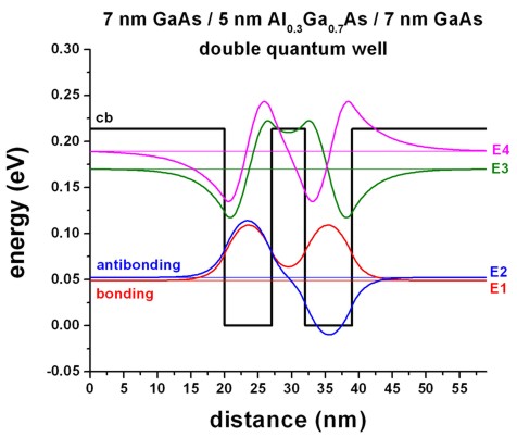
Fig. A shows a symmetric double quantum well where both wells have the
width 7 nm including the wave functions of the lowest confined states.
If the barrier between these two wells had been very large, both wells would
have had a ground state at 50.4 meV.
However, due to the small barrier, coupling between these two wells becomes
possible, and the two lowest states form a bonding
and an antibonding state, whereas the
bonding state now has a reduced energy of 48.7 meV
and and the antibonding state has an increased energy of
52.1 meV.
Fig. B shows a nonsymmetric double QW where the right QW has a width
of 12.5 nm.
In this case, the ground state can be found
in the larger well, the second state in the
7 nm QW, whereas the third eigenstate is
again localized in the larger well.
Here, no bonding or antibonding states exist.
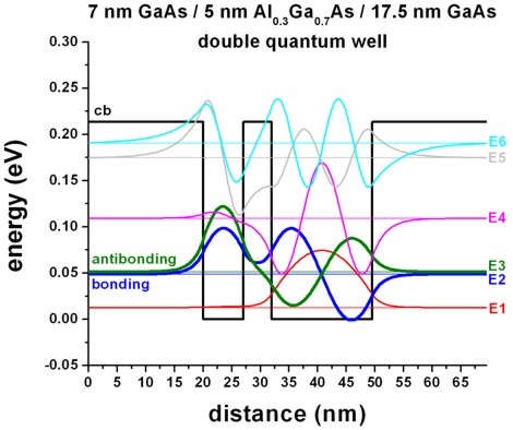
Fig. C shows a nonsymmetric double QW where the right QW has a width
of 17.5 nm.
In this case, the ground state can be again
found in the larger well (similar to Fig. B), but this this time, the third
state of Fig. B moves down in energy (compare with Fig. B) and couples to the 7
nm ground state (left well, compare with Fig. B). This coupling leads to the
formation of a bonding and an
antibonding states.
Fig. D shows a nonsymmetric double QW where the right QW has a width
of 25 nm.
In this case, the ground state and the
second state can be found in the larger well,
whereas the third eigenstate is localized in
the smaller (7 nm) well. The forth eigenstate
is localized in the larger well. Again, no bonding or antibonding states exist.
Now by looking at these figures, the anticrossing behavior and the plateaus
at 50.4 meV of the energy level scheme (see Fig. above) can be clearly
understood.
 |
|
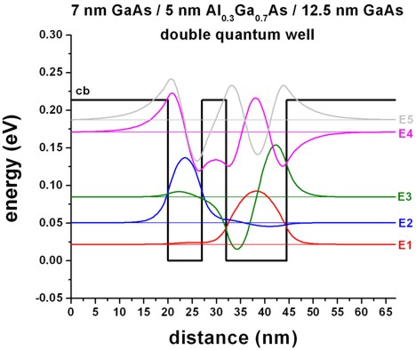 |
Fig. A
|
|
Fig. B
|
 |
|
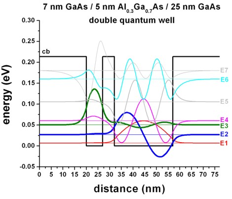 |
Fig. C
|
|
Fig. D
|
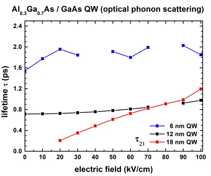
Biased double quantum well
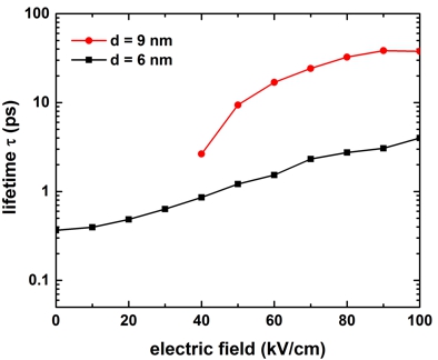
-> 1DGaAs_AlGaAs_DoubleQW_LifetimeFig12_field.in
The following figure shows the lifetime of the 2 ==> 1
transition ("ground state of left quantum well to ground state of right quantum
well transition") as a function of electric field.
The variable d is the thickness of the left well and the barrier region. The
right well is assumed to have the same thickness as the left quantum well, i.e.
d/2.
The variable d can be varied easily by making use of the variable
 %QWBarrierThickness = 6
! (DisplayUnit:nm) (ListOfValues:6,9)
There seems to be qualitative agreement to Fig. 12 of the paper by
[FerreiraBastard1989].
For d = 9 nm, the LO phonon emission is forbidden for electric fields smaller
than ~ | 40 kV/cm | because the transition energy is smaller than the LO phonon
energy of 36 meV.
|