nextnano3 - Tutorial
next generation 3D nano device simulator
1D Tutorial
Schottky barrier
Author:
Stefan Birner
-> 1DSchottky_barrier_GaAs.in
-
input file for the nextnano3 and nextnano++ software
(1D simulation)
-> 2DSchottky_barrier_GaAs.in
-
-> 1DSchottky_barrier_GaAs_ohmic.in
-
-> 1DSchottky_barrier_GaAs_SchottkyBarrier0V.in -
-> 1DSchottky_barrier_GaAs_surface_density.in -
-> 1DSchottky_barrier_GaAs_surface_states_acceptor.in -
These input files are included in the latest version.
Schottky barrier
-> 1DSchottky_barrier_GaAs.in

-> 2DSchottky_barrier_GaAs.in

-> 1DSchottky_barrier_GaAs_ohmic.in

-> 1DSchottky_barrier_GaAs_SchottkyBarrier0V.in
When a metal is in contact with a semiconductor, a potential barrier
is formed at the metal-semiconductor interface.
In 1938, Walter Schottky suggested that this potential barrier arises due to
stable space charges in the semiconductor.
At thermal equilibrium, the Fermi levels of the metal and the semiconductor
must coincide.
There are two limiting cases:
- a) Ideal Schottky barrier:
- metal/n-type semiconductor: The barrier height
phiB is the difference of the
metal work function phiM and the electron affinity (chi) in the
semiconductor.
e phiB
= e ( phiM - chis )
- metal/p-type semiconductor: The barrier height
phiB,p is given by:
- e phiB,p
= e ( phiM - chis ) -
Egap
- b) Fermi level pinning: If surface states on the semiconductor
surface are present: The barrier height is determined by the property of the
semiconductor surface and is independent of the metal work function
Consequence: The Schottky barrier sets a (Dirichlet) boundary condition for
the electrostatic potential, i.e. the solution of the Poisson equation in the
semiconductor, because the conduction and valence band edge energies are in a
definite energy relationship with the Fermi level of the metal.
The Schottky barrier model implemented in nextnano³ is basically a
Fermi level pinning and does not take into account the work function of the
metal: The barrier height is independent of the metal work function and is
entirely determined by the surface states and the doping.
$poisson-boundary-conditions


 poisson-cluster-number   = 1


 region-cluster-number    = 1

 ! boundary-condition-type  = ohmic
!
ohmic contact
 boundary-condition-type  = schottky
!
 contact-control          =
voltage


 applied-voltage          =
0.0        ! [V]


 schottky-barrier         =
0.53       ! [V]
The n-type donor concentration in GaAs has been taken to be 1 x 10¹⁸
cm-3 (fully ionized).
The temperature is set to 300 K.
The following figure shows the conduction band edge profile for n-type GaAs
in equilibrium with
- a Schottky barrier of 0.53 V, i.e. the conduction band edge is
pinned 0.53 eV above the Fermi level (which is at 0 eV)
- a Schottky barrier of 0 V
- an ohmic contact
at 10 nm.
(The contact region is from 0 nm to 10 nm but no equations are solved inside
the contact region.)
Note that in equilibrium the Femi level
is constant and equal to 0 eV in the whole device.
If the semiconductor is doped, the conduction and valence band edges are shifted
with respect to this Fermi level, i.e. relative to 0 eV and are thus dependent
on doping.
This is a bulk property and independent of surface effects, like ohmic contacts
or Schottky barrier height (see right part of the figure).
At the left boundary, however, the band profile is affected by the type of
contact.
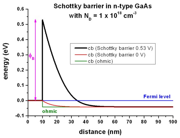
Note that a Schottky barrier of 0 V is not (!) equivalent to an ohmic
contact.
An ohmic contact corresponds to a Neumann boundary condition for the
Poisson equation (i.e. derivate of electrostatic potential = 0 (constant
electrostatic potential), i.e. flat band condition which is equivalent to
electric field = 0).
A Schottky barrier phiB is a
Dirichlet boundary condition for the Poisson equation, i.e. the value of the
conduction band edge at the boundary is fixed with respect to the
Fermi level: Ec – EFermi = e
phiB
(In this particular example, an artificial Schottky barrier of -0.04184
V would be equivalent to an ohmic contact, (i.e. flat band condition), but only
for the same temperature and the same doping concentration.)
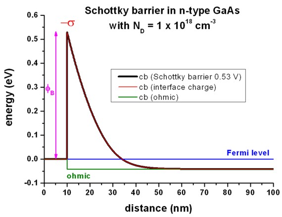
Interface charges (surface states)
-> 1DSchottky_barrier_GaAs_surface_density.in
Instead of specifying a Schottky barrier, the user can alternatively specify
a fixed surface charge density.
 $material-interfaces


  interface-number
= 1
!
sigma
  apply-between-material-numbers = 1 2
!
  state-numbers
= 1
! 1 =
 $end_material-interfaces


 $interface-states

  state-number
= 1
!
  state-type
= fixed-charge  !
  interface-density
= -2.7675e12    ! -2.7675 * 1012
[|e|/cm2]

 !interface-density
= 0.0
!       0 * 1012 [|e|/cm2]

 $end_interface-states
The following figure shows that the red curve
("ohmic" contact with interface charge density sigma (surface states) of -2.7675
* 1012 |e|/cm2 = -4.4340 * 10-3
C/m2 is equivalent to the black curve (Schottky barrier of
0.53 eV).
A sheet charge density of -2.7675 * 1012
cm-2 corresponds to a volume charge of -2.7675 * 1020 cm-3
if one assumes this charge to be distributed over a grid spacing of 0.1 nm.
In this case, the interface charge density corresponds to a Neumann boundary
condition for the derivative of the electrostatic potential phi:
dphi / dx = - Fx = constant /= 0, where Fx is
the electric field component along the x direction.
Fx is related to the interface charge as follows: Fx =
sigma / (epsilon0 epsilon) where epsilon0 is the
permittivity of vacuum and epsilon is the dielectric constant of the
semiconductor.
In this example (epsilon = 12.93 for GaAs), Fx = 387.3 kV/cm.
 static-dielectric-constants = 12.93  12.93
12.93
The output for the electric field (in units of [kV/cm]) can be found in this file:
band_structure/electric_field.dat
The output for the interface densities can be found in this file:
densities/interface_densitiesD.txt


   -----------------

   INTERFACE CHARGES

   -----------------


   Interface number 1 at position 10 nm

   interface charge: -4.434023546775000E-003 C / m^2

   interface charge: -2.76750000000000
1E12 e/cm^2
Surface states - Acceptors
-> 1DSchottky_barrier_GaAs_surface_states_acceptor.in
Instead of specifying a Schottky barrier, the user can alternatively specify
a density of acceptor surface states (p-type doping).
Essentially, this can be done by specifying a p-type doping region that is
very thin, i.e. the doping is specified only on one grid point.
In this example, we use a doping area of 0.1 nm at the surface that we dope
p-type with a volume density of 276.75 * 1018 cm-3.
This corresponds to a sheet charge density of 2.7675 * 1012 cm-2
where we assume the states to be fully ionized.
$doping-function

   ...

   doping-function-number      =
2
!

   impurity-number
= 2
 !
properties of this impurity type have to be specified
below
   doping-concentration        =
276.75
! 276.75 * 10^18 cm^-3

   only-region
= 10.0    10.1  ! [nm]  xmin
xmax


$end-doping-function


$impurity-parameters

   ...


!---------------------------------------------------------------------------------

   ! 'p-type' means a negative background
charge density of ionized acceptors NA-.


!---------------------------------------------------------------------------------

   impurity-number
= 2
!

   impurity-type
= p-type
!

   number-of-energy-levels     =
1
!

   energy-levels-relative      =
-1000.0
! [eV]
   degeneracy-of-energy-levels = 4
! 2
for n-type,
4 for p-type
$end_impurity-parameters
The results are the same as shown in the figure above for the interface
charges.
|