|
| |
nextnano3 - Tutorial
next generation 3D nano device simulator
1D Tutorial - Part 6
Piezoelectric fields due to strain (Quantum well)
Information on strain can also be found in the
FAQ
section and in the strain tutorial.
Author: Stefan Birner
If you want to obtain the input files that are used within this tutorial, please
check if you can find them in the installation directory.
If you cannot find them, please submit a
Support Ticket.
->
1Dpiezo_Al0.70In0.30As_In0.53Ga0.47As_100_nn3_growth_along_z_direction.in -
input file for the nextnano3 software
1Dpiezo_Al0.70In0.30As_In0.53Ga0.47As_311_nn3_growth_along_z_direction.in - input file for the nextnano3 software
1Dpiezo_Al0.70In0.30As_In0.53Ga0.47As_100_nn3.in / *_nnp.in - input file for the nextnano3 and nextnano++ software
1Dpiezo_Al0.70In0.30As_In0.53Ga0.47As_311_nn3.in / *_nnp.in -
1Dpiezo_Al0.33In0.67As_In0.32Ga0.68As_111_nn3.in / *_nnp.in -
Input files for nextnano.MSB and nextnano.NEGF software for this
tutorial are also available.
Piezoelectric fields
Piezoelectricity is due to the ionicity of III-V semiconductor compounds.
Si
and Ge have purely covalent bonds whereas the bonds of III-V compounds are
partially ionic (heteropolar) because the electrons spend on average more time
next to the (negatively charged) anions.
Zinc-blende structures are piezoelectric materials. Off-diagonal strain
tensor components (j≠k)
induce a polarization given by
Pis = 2 e14 epsilonjk
(epsilon = strain tensor)
where Ps is the induced polarization, e14 is
the piezoelectric constant and epsilonjk is a symmetrized
strain component.
However, diagonal strains (epsilonxx, epsilonyy, epsilonzz) do not
induce a polarization (i.e. e11=0).
A strained layer superlattice with a [001] growth direction will induce only
diagonal strains; but with any other growth direction, off-diagonal strains also
occur.
Thus [001]-growth axis strained-layer heterostructures will not have
strain-induced polarization fields, but strained-layer heterostructures with any
other growth direction will have these polarization fields.
Because one of the constituent materials is in biaxial tension and the other is
in biaxial compression, the polarization vector changes sign at the interface.
For a [111] growth axis, Ps is parallel to the growth axis,
for a [110] growth axis, Ps is in the interface plane; for
a [001] growth axis, Ps vanishes.
For a general growth axis,
Ps has components both parallel and perpendicular to the
growth axis.
The resulting interface charge density is given by
rho = - div Ps.
==> Text taken from D.L. Smith, C. Mailhiot, Rev.
Mod. Phys. 62 (1), 173 (1990)
Thus we want to test this on a quantum well structure consisting of Ga0.47In0.53As
(quantum well) and AlxIn1-xAs (barrier).
We will try 3 growth directions for Al0.70In0.30As.
- [001] - no strain-induced polarization fields (E=0)
- [011] - polarization vector Ps lies
in the interface plane
- [111] - polarization vector Ps is perpendicular to
interface and parallel to growth direction
(A superlattice grown in [111] direction has a different point group symmetry,
namely C3v, than [001] growth which is D2d.)
We will also try growth direction [111] with different alloy compositions
for the barrier resulting in different piezoelectric constants for each barrier
material.
- Al0.63In0.37As
- Al0.33In0.67As
Ga0.47In0.53As/Al0.48In0.52As is
lattice matched to InP.
By proper
choice of alloy composition of AlxIn1-xAs, one can subject
this layer to either tensile or compressive strain when grown
pseudomorphic on InP leading to a splitting in light hole (lh) and heavy hole (hh)
bands and also changing their order.
Okay, let's compare the growth directions for a Ga0.47In0.53As
- Al0.70In0.30As quantum well.
|
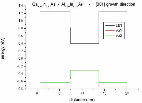
- along [001] direction
==>
		1Dpiezo_Al0.70In0.30As_In0.53Ga0.47As_100_nn3_growth_along_z_direction.in
Splitting due to strain: The heavy hole band (vb1)
is lower than the light hole band (vb2) of Al0.70In0.30As
(barrier) due to tensile strain.
Due to the [001] growth direction, no piezoelectric charges are present.
|
|
 |
Conduction
and
valence bands
along [001] |
|
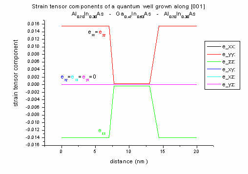 |
Strain
along [001] |
|
[001] growth direction: The well region is lattice matched to
InP, therefore strain is zero. Only the barrier region is subject to
strain. The off-diagonal strain tensor components are all zero (exy=exz=eyz=0)
as we have [001] growth direction. Al0.70In0.30As has
a smaller lattice constant than the substrate material InP (lattice mismatch
1.55 %) leading to tensile strain.
In 1D strain can be calculated analytically along [001] growth direction:
(a = lattice constant, c11, c12 = elastic constants):
Biaxial strain (in plane of interface):
exx = eyy
= ( asubstrate - alayer ) / alayer = 0.0155 (1.55 % lattice mismatch)
Uniaxial strain (perpendicular to interface):
ezz = - 2 (c12/c11) exx
= - 0.014
For [001] growth direction, crystal and simulation system coincide. Thus the
strain given in the crystal coordinate system is equal to the strain given
in the simulation system.
|
|
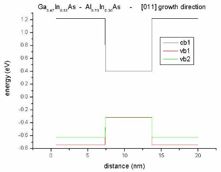
- along [011] direction
changes in input file:
hkl-z-direction-zb = 0 1 1 ! Miller indices of
z
coordinate axis [0 0 1]
hkl-y-direction-zb = 0 1 -1 !
There's no effect due to piezoelectric charges as the polarization vector
is directed along the interface (perpendicular to growth direction).
|
|
 |
Conduction
and
valence bands
along [011] |
|
 |
Strain
along [011] |
|
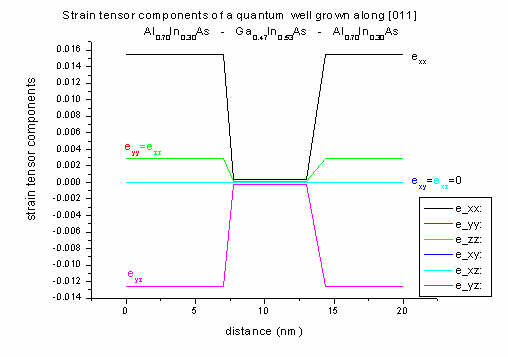
[011] growth direction: The well region is lattice matched to InP,
therefore strain is zero. Only the barrier region is subject to strain.
exx again can be calculated analytically as above with the same
result. The off-diagonal strain components that include x are zero (exy=exz=0).
Due to shear strain in the (y,z) plane, eyz is not zero.
Al0.70In0.30As has a smaller lattice constant than the
substrate material InP (lattice mismatch 1.55 %) leading to tensile strain.
In 1D layered heterostructures, strain can be calculated analytically along [011] growth direction (see
FAQ section). The strain tensor components can
be printed out with respect to the crystal
coordinate system and simulation coordinate
system (see keyword
$output-strain).
For [011] growth direction, crystal and simulation system do not
coincide anymore. Thus the strain given in the crystal coordinate system is
not equal to the strain given in the simulation system anymore.
In the simulation system all off-diagonal components of the strain tensor
are zero (exy,sim=exz,sim=eyz,sim=0) and eyy,sim=ezz,sim.
|
|
- along [111] direction
changes in input file:
hkl-z-direction-zb = 1 1 1 ! Miller indices of z
coordinate axis [1 1 1]
hkl-y-direction-zb = 0 1 -1 !
The polarization vector due to piezoelectric charges is directed along the
[111] growth direction leading to a slope in the conduction and valence
bands.
|
|
 |
Conduction
and
valence bands
along [111] |
 |
Strain
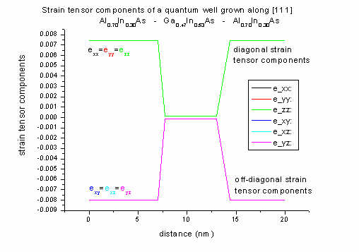
along [111] |
[111] growth direction: The well region is lattice
matched to InP, therefore strain is zero. Only the barrier region is subject
to strain.
In 1D strain can be calculated analytically along [111] growth direction (see
FAQ section).
The off-diagonal strain components (shear strain) are all equal (exy=exz=eyz).
Al0.70In0.30As has a smaller lattice constant than the
substrate material InP (lattice mismatch 1.55 %) leading to tensile strain.
For [111] growth direction, crystal and simulation system do not coincide
either. Again, the strain given in the crystal coordinate system is not
equal to the strain given in the simulation system.
In the simulation system all off-diagonal components of the strain tensor
are again zero (exy,sim=exz,sim=eyz,sim=0)
and eyy,sim=ezz,sim.
Note: For [321] growth direction eyz,sim=0 but all other
off-diagonal compontents are not zero anymore. In the simulation system, for
any growth direction, eyy,sim=ezz,sim=exx,sim[111]=exx,sim[hkl].
For the pictures above, the strain tensor components are plotted with
respect to the
crystal coordinate system, not simulation coordinate system.
|
|
| |
|
| Discussion of piezoelectric field |
|
| For the [111] case the polarization vector is along [111].
As expected we get an electric field. For [011] the polarization vector
lies in the interface (no resulting E field) and for [001] there isn't any
polarization verctor. |
| |
|
([111] growth: If you change the piezoelectric constant e14
in the database_nn3.in file
to zero, you won't get a slope and the picture looks as for the [001] case.
If you change the signs of these constants from negative to positive, the
slope would be reversed. The direction depends on the sign, e.g.
positive from In (cation) to As (anion) along [111].)
You can also switch of piezoelectricity using the flag piezo-constants-zero =
yes in
$numeric-control.
|
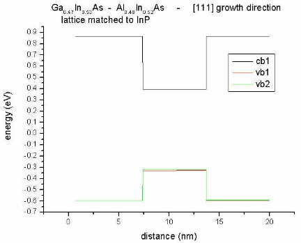
- along [111] direction
Again we take the [111] direction but this time we take lattice matched Ga0.47In0.53As
and Al0.48In0.52As (lattice matched to InP) herby
avoiding any strain. Thus we do not get any heavy hole/light hole
splitting. Without strain we even don't get piezoelectric charges and thus
no slope.
|
|
 |
|
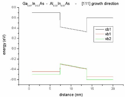
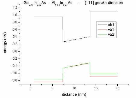
- along [111] direction
Here, we change the alloy composition of the barrier.
(strain calculation: pseudomorphic on InP substrate:
homogeneous-strain)
- biaxial compression for Al0.33In0.67As
- biaxial tension for Al0.63In0.37As
- still no strain for the well
Now the electric field resulting from piezoelectric charges changes its direction
in the two cases.
The heavy hole (vb1) / light hole (vb2)
splitting is also different in these two cases!
|
|
 |
biaxial compression
for
Al0.33In0.67As |
|
 |
biaxial tension for:
Al0.63In0.37As |
|
|
|
- along [111] direction
Our substrate is InP.
We now combine compressive (Ga0.32In0.68As) and
tensile (Al0.63In0.37As) strain. Now for
both materials, heavy hole (vb1) and light
hole (vb2) bands split but into opposite
directions.
|
|
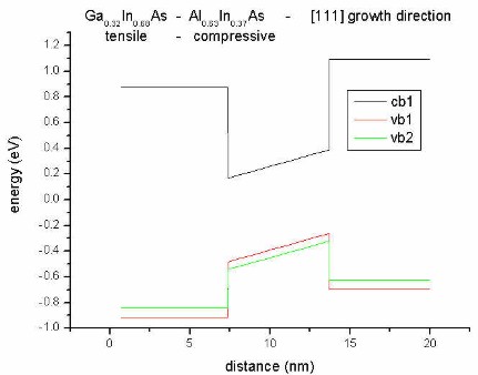 |
biaxial tension for:
Al0.63In0.37As
(barrier)
biaxial compression
for:
Ga0.32In0.68As
(well) |
- along [111] direction
==> 1Dpiezo_Al0.33In0.67As_In0.32Ga0.68As_111_nn3.in
Our substrate is InP.
We now combine tensile (Ga0.68In0.32As)
and compressive (Al0.33In0.67As) strain. Now for
both materials, heavy hole (vb1) and light
hole (vb2) bands split again but into
opposite directions and into opposite directions compared to the previous
pictures.
|
|
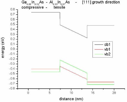 |
biaxial compression for:
Al0.33In0.67As
(barrier)
biaxial tension
for:
Ga0.68In0.32As
(well)
|
|
|
|
Step 1: Quantum well structure - Piezoelectric fields
- The structure is grown pseudomorphic on an InP substrate.
- We perform a one-dimensional simulation.
- Just a reminder: If you need additional information about the keywords and
their specifiers, you can look it up
here.
- The heterostructure looks like this:
!    barrier
  well
  barrier
!       1
  2
  3
!
! Al(x)In(1-x)As    In(x)Ga(1-x)As
  Al(x)In(1-x)As
!       7
  6
  7           nm
!___________________________________________________
- The structure has no doping.
- Output
- The band structure will be saved into the directory band_profile/
- The densities will be saved into densities/
- The strain will be saved into strain/
- The material parameters will be saved into material_parameters/
- You should be able to modify the appropriate lines in the input file
1Dpiezo.in
in order to reproduce the results shown above.
	 $domain-coordinates
  ...
 $end_domain-coordinates


 $alloy-function
  ...
 $end_alloy-function
|