|
| |
nextnano3 - Tutorial
next generation 3D nano device simulator
1D Tutorial
pn-junction
Author:
Stefan Birner
-> GaAs_pn_junction_1D_nn3.in / *_nnp.in -
input file for the nextnano3 and nextnano++ software
-> GaAs_pn_junction_1D_QM_nn3.in
-
-> GaAs_pn_junction_2D_nn3.in / *_nnp.in -
-> GaAs_pn_junction_3D_nn3.in / *_nnp.in -
-> GaAs_pn_junction_1D_ForwardBias_nn3.in / *_nnp.in -
-> GaAs_pn_junction_2D_ForwardBias_nnp.in -
input file for the nextnano++ software
-> GaAs_pn_junction_3D_ForwardBias_nnp.in -
These input files are included in the latest version.
pn-junction
-> GaAs_pn_junction_1D_nn3.in / *_nnp.in - input file for the nextnano3 and nextnano++ software
This tutorial aims to reproduce figure 3.1 (p. 51) of
Joachim Piprek's
book "Semiconductor
Optoelectronic Devices - Introduction to Physics and Simulation" (Section 3.2 "pn-Junctions").
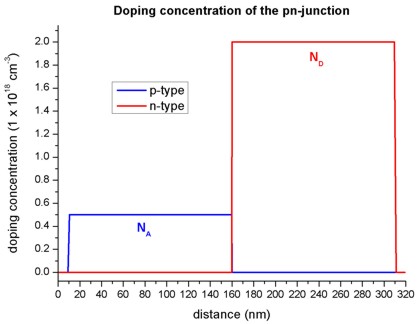
Doping concentration
- The structure consists of 300 nm GaAs.
At the left and right boundaries, metal contacts are connected to the GaAs
semiconductor (i.e. from 0 nm to 10 nm, and from 310 nm to 320 nm).
The structure is p-type doped from 10 nm to 160 nm and n-type doped from 160
nm to 310 nm.
- The following figure shows the concentration of donors and acceptors of
the pn-junction.
In the p-type region between 10 nm and 160 nm, the number of acceptors NA
is 0.5 x 1018 cm-3.
In the n-type region between 160 nm and 310 nm, the number of donors ND
is 2.0 x 1018 cm-3.
Carrier concentrations
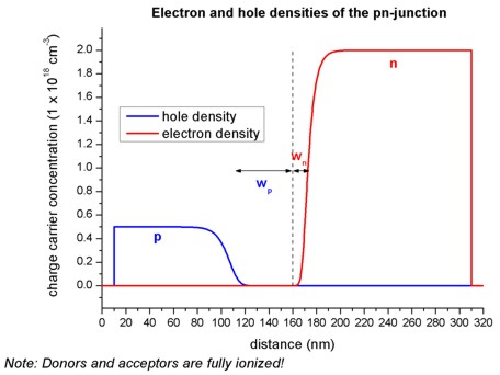
- The equilibrium condition for a pn-junction is achieved by a small
transfer of electrons from the n region to the p region, where they recombine
with holes. This leads to a depletion region (depletion width = wp
+ wn), i.e. the region around the pn-junction only has very few
free carriers left.
- The following figure shows the electron and hole densities and the
depletion region around the pn-junction at 160 nm. Here, we assumed that all
donors and acceptors are fully ionized.
Net charges (space charge)
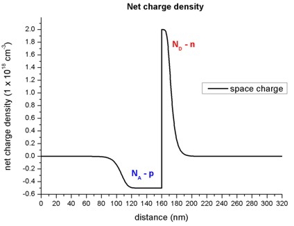
- In the depletion region, a net charge results from the ionized donors ND
and ionized acceptors NA.
- The following figure shows the net charge density of the pn-junction.
Electric field
- The slope of the electric field is proportional to the net charge (Poisson
equation), thus the extremum of the electric field is expected to be at the
pn-junction.
- In regions without charges, the electric field is zero.
- The following figure shows the electric field of the pn-junction.
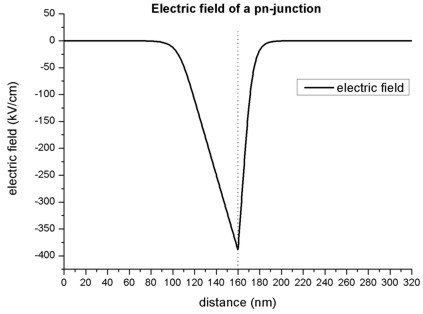
The extremum of the electric field Fmax (at 160 nm) can be
approximated as follows:
Fmax = - e NA wp / (epsilon epsilon0)
= - 6.997 x 10¹⁴ V/m2 wp = 387 kV/cm
= - e ND wn /
(epsilon epsilon0) = - 2.799 x 10¹⁵ V/m2 wn
= 386 kV/cm
where
e = 1.6022 x 10⁻¹⁹ As
epsilon = 12.93 (dielectric constant of GaAs)
epsilon0 = 8.854 x 10⁻¹² As/(Vm)
NA = 0.5 x 1018 cm-3
ND = 2.0 x 1018 cm-3
wp = 55.3 nm
wn = 13.8 nm
Electrostatic potential, conduction and valence band edges
- In regions, where the electric field is zero, the electrostatic potential
is constant.
- The electrostatic potential phi determines the conduction and valence band
edges:
Ec = Ec0 - e phi
Ev = Ev0 - e phi
- The following figure shows the conduction and valence band edges, the
electrostatic potential and the Fermi level of the pn-junction.
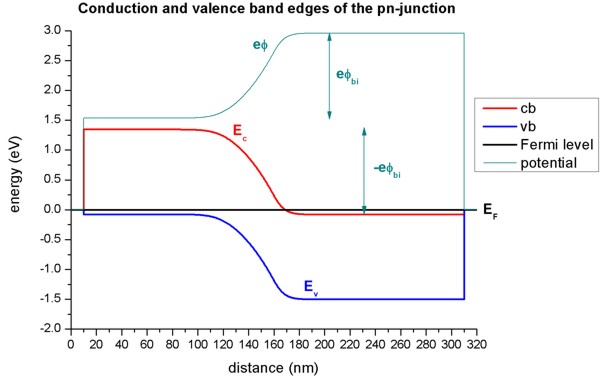
Without external bias (i.e. equilibrium), the Fermi level EF is
constant (EF = 0 eV).
The built-in potential phibi was calculated by nextnano³ to
be equal to 1.426 V.
It can be approximated as follows:
phibi = Fmax (wp + wn)
/ 2
Assuming Fmax = 387 kV/cm, this would indicate for the depletion
width: wp + wn = 73.7 nm.
To allow for a constant chemical potential (i.e. constant Fermi level EF),
a total potential difference of -e phibi is required.
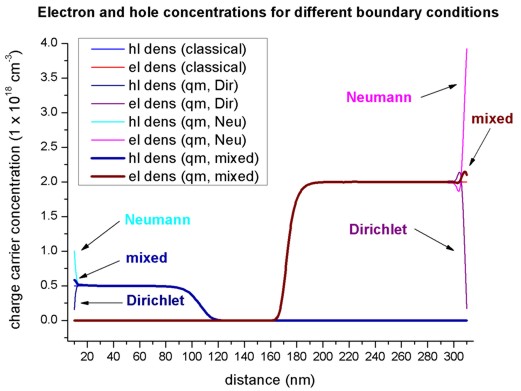
Quantum mechanical calculation
-> GaAs_pn_junction_1D_QM_nn3.in
- Here, instead of calculating the densities classically, we solve the
Schroedinger equation for the electrons, light and heavy holes in the
single-band approximation over the whole device. We calculate up to 300
eigenvalues for each band. Thus the electron and hole densities are calculated
purely quantum mechanically.
- The following figure shows the electron and hole concentrations for the
classical and quantum mechanical calculations. For the QM calculations,
different boundary conditions were used.
- Dirichlet boundary conditions force the wave functions to be zero at
the boundaries, thus the density goes to zero at the boundaries which is
unphysically.
- Neumann boundary conditions lead to unphysically large values at
the boundaries.
- Mixed boundary conditions are in between.
(This feature is not supported any more.)
For the classical calculation, the densities at the boundaries are constant.
Nevertheless, in the interesting region around the pn-junction, all four
options lead to identical densities.
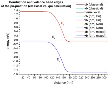
- The following figure shows the band edges of the pn-junction for the four
cases:
- classical calculation
- quantum mechanical calculation with Dirichlet boundary conditions
- quantum mechanical calculation with Neumann boundary conditions
- quantum mechanical calculation with mixed boundary conditions
(This feature is not supported any more.)
For all cases the band edges are identical in the area around the pn-junction.
Tiny deviations exist at the boundaries of the device.
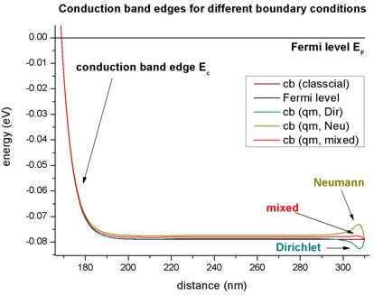
- This figure is a zoom into the right boundary of the conduction band edge.
On this scale, the tiny deviations for the different boundary conditions can
be clearly seen.
Nonequilibrium
- So-called "quasi-Fermi levels" which are different for electrons (EF,n)
and holes (EF,p) are used to describe nonequilibrium carrier
concentrations.
In equilibrium the quasi-Fermi levels are constant and have the same value for
both electrons and holes (EF,n = EF,p = 0 eV).
The current is proportional to the mobility and the gradient of the
quasi-Fermi level EF.
-> GaAs_pn_junction_1D_ForwardBias_nn3.in / _nnp.in -
input file for the nextnano³ software and nextnano++ software
2D/3D simulations
-> GaAs_pn_junction_2D_nn3.in / *_nnp.in - input file for the nextnano3 and nextnano++ software
-> GaAs_pn_junction_3D_nn3.in / *_nnp.in -
Input files for the same pn junction structure as in 1D, but this time for a
2D and 3D simulation are also available.
==> 2D: rectangle of dimension 320 nm x 200 nm
==> 3D: cuboid of dimension 320 nm x 200 nm x
100 nm
|