nextnano3 - Tutorial
next generation 3D nano device simulator
1D Tutorial
Carrier statistics of graphene sheets
Author:
Stefan Birner
If you are interested in the input files that are used within this tutorial,
please submit a support ticket.
-> 1D_graphene_intrinsic_Tsweep.in

-> 1D_graphene_intrinsic_1overTsweep.in

-> 1D_graphene_FermiLevel_sweep.in

-> 1D_graphene_FermiLevel_sweep_fluctuation.in
Carrier statistics of graphene sheets
Here, we calculate the intrinsic electron and hole densities in graphene as a
function of temperature,
and finally we calculate the carrier densities as a function of the position of
the Fermi level.
We recommend that you first get familiar with the tutorial:
Tight-binding band structure of graphene
This tutorial is based on the following paper:
[Fang2007]
"Carrier statistics and quantum capacitance of graphene sheets and ribbons"
T. Fang, A. Konar, H. Xing, D. Jena
Appl. Phys. Lett. 91, 092109 (2007)
We assume a linear energy dispersion E(k):
E(k) = +- hbar vF | k | = +- hbar
vF ( kx2 + ky2
)1/2
The Fermi velocity vF of the charge carriers in graphene is
defined as:
vF = 31/2 | gamma0 |
a / (2 hbar) ~= 0.98 * 106 m/s ~= 0.003 c
where a is the lattice constant of graphene (a = 0.24612 nm) and c is the velocity of light.
(vF is 300 times smaller than the speed of light.)
 lattice-constants = 0.24612 0.24612
0.67079 ! Graphene ! a,a,c [nm] a = graphene, c = graphite
gamma0 has to be specified via the input file. It is a
tight-binding parameter. (Usually it holds: -3 eV < gamma0
< -2.5 eV.)
 tight-binding-parameters =  0.0
! [Saito] [eV] E2p: site energy of the 2pz atomic
orbital (orbital energy)
-3.013 ! [Saito] [eV]
... ! ...
Assuming a linear energy dispersion, the linear density of states (DOS) is
given by:
gs gv
DOS (E) = ---------------------- | E |
2pi ( hbar vF )2
The spin degeneracy is gs = 2.
The valley degeneracy is gv = 2 (K and K' valleys).
To calculate the density, one has to integrate the linear DOS over the energy
(taking into account the Fermi-Dirac distribution function).
Inside the code this involves the numerical evaluation (approximation) of the
Fermi-Dirac integral of order 1 (multiplied with the Gamma prefactor which
equals 1 for FD integral of order 1).
The precision can be adjusted via the input file:
 ! fermi-function-precision = 1e-6
!
(default)
fermi-function-precision = 1e-14 !
The Fermi-Dirac integral FFD,1 of order 1 (multiplied
with the Gamma prefactor which equals 1 for FD integral of order 1) is
evaluated to be equal to pi2/12 in case its argument is zero.
 !
FFD,1 = 0.822467074217074
(==> fermi-function-precision = 1e-6)

 !            FFD,1
= 0.822467033424114   (==>
fermi-function-precision = 1e-14)

 ! ==> exact result: 0.822467033424113218 = pi2 / 12
Intrinisic carrier density
Under thermal equilibrium, and under no external perturbation (no applied
bias), the Fermi level is exactly in the middle of the (zero) band gap at EF
= 0 eV (Dirac point).
The intrinsic density is then given by ni = pi = pi / 6
* ( kT / (hbar vF) )2.
It depends quadratically on the temperature. At room temperature (T = 300 K),
the intrinsic density is about ni = 8.5 * 1010 cm-2.
Intrinisic carrier density as a function of T
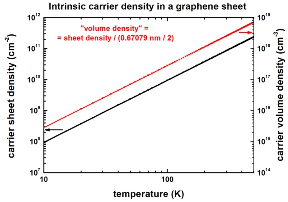
-> 1D_graphene_intrinsic_Tsweep.in
The following figure shows the intrinsic carrier sheet and volume density as
a function of temperature.
The carrier density is the same for electrons and holes.
The calculated volume density can be found in this file:
sweep_temperature.dat
(Note: nextnano³ internally deals with volume densities.)
To obtain the sheet density, we divided the volume density by the height of one
graphene layer which is the graphite height (i.e. lattice constant of graphite
along c direction) divided by 2. (==> graphene height =
0.67079 / 2 = 0.335395 nm)
We used the following settings:
  flow-scheme = 13
!
vary temperature T (temperature sweep)
 $global-parameters

  lattice-temperature
= 5.0    ! 5 Kelvin

  temperature-sweep-active
= yes    ! 'yes'
/ 'no'

  temperature-sweep-step-size       =
5.0    ! [K]

  temperature-sweep-number-of-steps = 100
!

  data-out-every-nth-step
= 50     !
Intrinisic carrier density as a function of 1/T
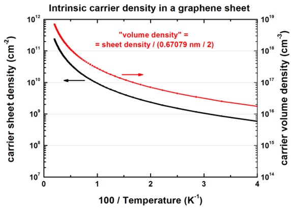
-> 1D_graphene_intrinsic_1overTsweep.in
The following figure shows the intrinsic carrier sheet and volume density as
a function of 100 / temperature.
The carrier density is the same for electrons and holes.
The calculated volume density can be found in this file:
sweep_temperature.dat
We used the following settings:
  flow-scheme = 14
!
vary temperature as 1000/T (temperature sweep)
 $global-parameters

  lattice-temperature
= 500.0  ! 500 Kelvin

  temperature-sweep-active
= yes    ! 'yes'
/ 'no'

  temperature-sweep-step-size       =
-5.0   ! [K]

  temperature-sweep-number-of-steps = 100
!

  data-out-every-nth-step
= 50     !
Carrier densities as a function of the position of the Fermi level
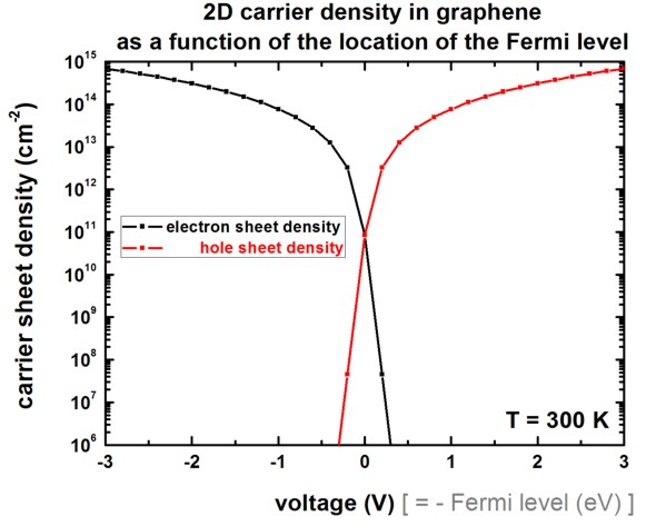
-> 1D_graphene_FermiLevel_sweep.in
The following figure shows the 2D electron and hole carrier sheet densities
as a function of the applied voltage (i.e. position of the Fermi level) at room
temperature.
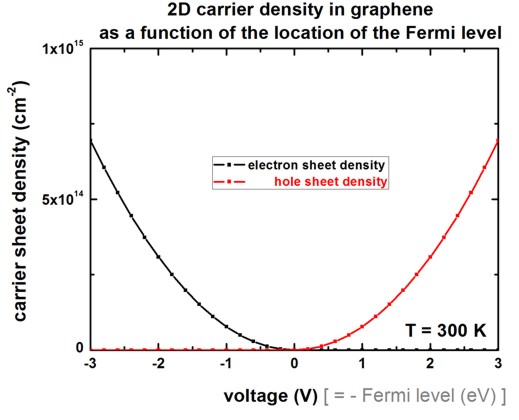
The same figure as above but on a linear scale.
The same figure as above but this time a zoom into the small voltage region.
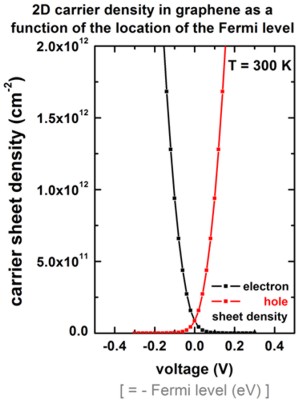
This figure can be compared to Fig. 3 (right) of [Fang2007].
Note that our figure only includes the graphene layer but no oxide.
To plot this graph, we used the following settings:
flow-scheme = 0 !
	0 =
do nothing- Here, we apply a trick!
device length = 0.335395 nm = 0.67079 nm / 2 where 0.67079 is the lattice
constant in graphite
z-coordinates = 0.0 0.335395 !
[nm]
Having such a device length, one can use the following files to plot the
above graph:
- densities/int_el_dens.dat: integrated volume density
[cm-3] over whole device ==> electron sheet density in units of
[cm-2]
- densities/int_hl_dens.dat: integrated volume density
[cm-3] over whole device ==> hole
sheet density in units of [cm-2]
Capacitance
The derivative of the total charge with respect to the voltage (i.e. local
channel electrostatic potential) is shown in the following figure.
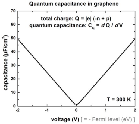
The figure has been generated by adding the electron sheet density
-n and the hole sheet density
p (taking into account that the electron
density is negative) for each voltage point. Multiplied by the electron charge
|e|, this gives the electron density in units of [As/cm2]: Q =
-n + p
Then plot Q vs. V.
A program like Origin allows to calculate the derivate ("Differentiate")
of the Q(V) plot leading to the quantum capacitance
CQ = dQ / dV.
The following files contained the data that were used in this plot.
- densities/int_el_dens.dat
- densities/int_hl_dens.dat: integrated volume density
[cm-3] over whole device ==> hole
sheet density p in units of [cm-2]
In order to get reasonable values for the capacitance at around V = 0 V, we
calculated the densities by increasing the voltage in steps of 50 mV.
 $voltage-sweep

  ...

  step-size = 0.050  ! 0.050 V = 50 mV
For the capacitance, it is easier to use the file
- densities/int_space_charge_dens.dat: integrated volume
space charge density
[cm-3] over whole device which is the sum of
the negative electron sheet density
n and
the positive hole sheet density p in units of
[cm-2]
and then build the derivative of this file with a
program like e.g. Origin.
Capacitance with potential fluctuations
-> 1D_graphene_FermiLevel_sweep_fluctuation.in
In the paper
Measurements and microscopic model of quantum capacitance in graphene
H. Xu et al.,
Applied Physics Letters 98, 133122 (2011)
it was assumed that a real graphene layer differs from a perfect graphene
layer due to potential fluctuations that obey a Gaussian distribution.
The derivative of the total charge with respect to the voltage (i.e. local
channel electrostatic potential) is shown in the following figure for 5
different values of the potential fluctuation.
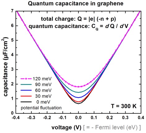
Here we show how potential energy fluctuations can be added to the graphene
layer.
$numeric-control

   ...

   graphene-potential-fluctuation = 0.120
 ! [eV]
potential energy fluctuation of graphene layer
0.001 ! [eV]
3.0 ! []
Following the paper of Xu et al. we used a Fermi velocity of 1.15 * 106
[m/s] for the above figure where potential fluctuations were included.
 %FermiVelocity = 1.15e6
! Fermi velocity corresponding to gamma0 =
-3.551289126 eV   (DisplayUnit:m/s)

!%FermiVelocity =
0.975687948e6 ! Fermi velocity corresponding to gamma0 =
-3.013 eV
(DisplayUnit:m/s)

 %constant      =
323826.0697
!
(DisplayUnit:m/seV)

 %gamma0
= - %FermiVelocity / %constant ! [eV] gamma0:
(DisplayUnit:eV)
 tight-binding-parameters =
...


! -3.013   ! [Saito] [eV] gamma0:
C-C transfer energy (nearest-neighbor, nn)
%gamma0 !
[eV] gamma0:
...
Conclusion: For high gate voltages, potential fluctuations are negligible.
|