nextnano3 - Tutorial
next generation 3D nano device simulator
1D Tutorial
Si/SiGe MODQW (Modulation Doped Quantum Well)
Authors:
Stefan Birner
==> 1DSiGe_Si_Schaeffler_SemicondSciTechnol1997_nn3.in
-
input file for the nextnano3 software
==> 1DSiGe_Si_Schaeffler_SemicondSciTechnol1997_nnp.in -
These input files are included in the latest version.
Si/SiGe MODQW (Modulation Doped Quantum Well)
This tutorial aims to reproduce Fig. 11 of
F. Schäffler
High-Mobility Si and Ge structures
Semiconductor Science and Technology 12, 1515
(1997)
Step 1: Layer sequence
| |
width [nm] |
material |
strain |
doping |
|
| 1 |
|
Schottky barrier 0.8 eV |
|
|
|
| 2 |
15.0 |
Si cap |
strained w.r.t. Si0.75Ge0.25 |
|
|
| 3 |
22.5 |
Si0.75Ge0.25 layer |
|
|
|
| 4 |
15.0 |
Si0.75Ge0.25 doping layer |
|
2 x 1018 cm-3 (fully ionized) |
|
| 5 |
10.0 |
Si0.75Ge0.25 barrier (spacer) |
|
|
|
| 6 |
18.0 |
Si channel |
strained w.r.t. Si0.75Ge0.25 |
|
|
| 7 |
69.5 |
Si0.75Ge0.25 buffer layer |
|
|
|
| |
|
|
|
|
|
Step 2: Material parameters
The material parameters were taken from:
F. Schäffler
High-Mobility Si and Ge structures
Semiconductor Science and Technology 12, 1515
(1997)
The temperature was set to 0.1 Kelvin.
The Si layers are strained pseudomorphically with respect to a Si0.75Ge0.25
substrate (buffer layer).
Step 3: Method
Self-consistent solution of the Schrödinger-Poisson equation within single-band
effective-mass approximation (using ellipsoidal effective mass tensors) for both
Delta conduction band edges.
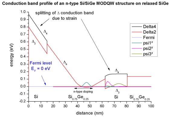
Step 4: Results
- The following figure shows the self-consistently calculated conduction
band profile and the lowest wave functions of an n-type Si/Si0.75Ge0.25
modulation doped quantum well (MODQW) grown on a relaxed Si0.75Ge0.25
buffer layer.
The strain lifts the sixfold degeneracy of the lowest conduction band (Delta6)
and leads to a splitting into a twofold (Delta2) and a fourfold
(Delta4) degenerate conduction band edge.
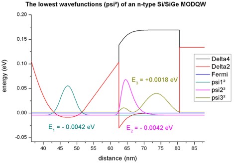
- The following figure shows the lowest three wave functions (psi²) of
the structure. Two eigenstates that have very similar energies and are occupied
(i.e. they are below the Fermi level) whereas the third eigenstate is not
occupied at 0.1 K.
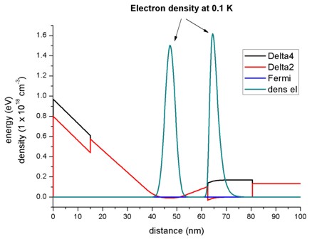
- The electron density (in units of 1 x 1018 cm-3) is
plotted in this figure. The lowest states in each channel are occupied, i.e. are
below the Fermi level.
The integrated electron densities are:
- in the parasiticSi0.75Ge0.25
channel: 0.75 x 1012 cm-2
- in the strained Si channel: 0.66 x 1012 cm-2
|