nextnano3 - Tutorial
next generation 3D nano device simulator
1D Tutorial
Piezoelectric field in InAs/GaAs QWs grown along the [111] orientation
Author:
Stefan Birner
If you want to obtain the input files that are used within this tutorial, please
check if you can find them in the installation directory.
If you cannot find them, please submit a
Support Ticket.
 -> 1DInAsQW_onGaAs111_piezo_11nm_nn3.in
/ *_nnp.in -
input file for the nextnano3
and nextnano++ software
-> 1DInGaAsQW_onGaAs111_piezo_2ndOrder_nn3.in / *_nnp.in -
 -> 1DInGaAsQW_onGaAs111_piezo_nn3.in
/ *_nnp.in -
Piezoelectric field in InAs/GaAs QWs grown along the [111] orientation
In this tutorial we study the effect of the piezoelectric field of an InAs QW
embedded between GaAs barrries.
Sign convention of the piezoelectric constant in zinc blende
materials
According to T. Ikeda [Fundamentals of piezoelectricity, Oxford Science
Publications, 1st ed., p. 53 (1990)] the sign of the piezoelectric
constant is taken as positive if a positive charge is induced in the positive
direction of the axis under a positive (tensile) stress.
In nextnano³ we define as the positive [111] direction the one from
cation (i.e. metal ion, e.g. Ga in GaAs) to anion (e.g. As in GaAs),
i.e. parallel to the Ga-As bond. In this case the
piezoelectric constant can be both positive (AlP, InP) and negative (AlAs, InAs,
GaAs). Note that this is the same definition as for wurtzite where the positive
[0001] direction is defined from cation to anion and also the same definition
that is used by the wafer manufacturers.
This definition has also been used in the article Piezoelectricity by
R. M. Martin, Physical Review B 5, 1607 (1972).
cation: positively charged ion, e.g. Ga3+
anion: negatively charged ion, e.g. As3-
This tutorial is based on the following paper:
[Bester]
Importance of Second-Order Piezoelectric Effects in Zinc-Blende
Semiconductors
G. Bester, X. Wu, D. Vanderbilt, A. Zunger
Physical Review Letters 96, 187602 (2006)
We use a 11 nm InxGa1-xAs quantum well embedded between
14 nm GaAs barriers on each side.
We employ periodic boundary conditions to the Poisson equation which is
equivalent to a 11 nm InGaAs / 28 nm GaAs superlattice.
The heterostructure is strained pseudomorphically with respect to GaAs
substrate, i.e. GaAs is unstrained, InGaAs is compressively strained.
InAs quantum well between GaAs
 -> 1DInAsQW_onGaAs111_piezo_11nm_nn3.in

    %AlloyContent =
1.0  ! InAs , alloy content In(x)Ga(1-x)As (DisplayUnit:)

    %QW_width
= 11.0 ! quantum well width
(DisplayUnit:nm)
Strain
For more information on strain, please have a look at this tutorial:
Strain and displacement tensors along different
growth directions
For a compressively strained InAs layer grown along the [111] direction on
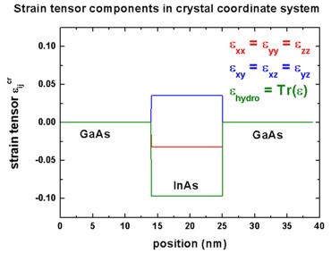
GaAs, we obtain the following strain tensor components:
- As GaAs is unstrained, all strain tensor components are zero in GaAs.
- In InAs, the strain tensors components with respect to the crystal
coordinate system are as follows:
epsxx = epsyy = epszz = -0.03219
(i.e. negative)
epsxy = epsxz = epsyz = 0.03533
(i.e. positive)
- The trace of the strain tensor is negative, i.e. the hydrostatic strain
epshydro = Delta V / V =
-0.09656 which is negative
as it should be for a compressed crystal.
Polarization and piezoelectric charge density
 -> 1DInAsQW_onGaAs111_piezo_11nm_nn3.in

    %QW_width =
11.0   ! quantum well width (DisplayUnit:nm)

    %InAs_e14 =
-0.045 ! 1st order piezoelectric coefficient e14 (InAs),
experimental value (DisplayUnit:C/m^2) (ListOfValues:-0.045,-0.115)
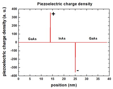
In a zinc blende crystal, the polarization with respect to the crystal
coordinate system is defined as P = e14 (2 epsyz
, 2 epsxz , 2 epsxy).
Consequently, in GaAs the polarization is zero because the strain tensor is
zero.
In compressively strained InAs, the polarization P is negative if e14
is negative (along the [111] direction) and because the off-diagonal strain
tensor components are positive.
In this example, we use the following experimentally determined piezoelectric
constants for bulk InAs:
We compare this value to the value as calculated by [Bester].
- InAs: e14 =
-0.115
C/m2 (However, we neglect
second-order terms.)
The piezoelectric charge density is definded as: rhopiezo =
- div P
P (GaAs) = 0
P (InAs) = negative
P (GaAs) = 0
==> left interface: rhopiezo = -
d/dz Pz = - [Pz(InAs) - Pz
(GaAs)] / (Delta_z) = positive value
==> right interface: rhopiezo = - d/dz Pz
= - [Pz(GaAs) - Pz (InAs)]
/ (Delta_z) = negative value
Consequently, for a compressively strained InAs QW, a positive piezo
charge density arises on the left interface, and a negative piezo charge
density at the right interface.
The piezoelectric interface charge densities are calculated to be:
Filename: densities/interface_densitiesD.txt
For InAs: e14 = -0.045
C/m2, the results are:
Interface number 1 at position 14.0000000000000 nm
piezoelectric charge: 5.506839895904100E-003 C/m^2
  piezoelectric charge:  3.43709934129674 1E12  |e| / cm^2


  Interface number 2 at position 25.0000000000001 nm
piezoelectric charge: -5.506839895904100E-003 C/m^2
piezoelectric charge: -3.43709934129674 1E12 |e| / cm^2
Piezoelectric potential
    %InAs_e14 =
-0.045 ! 1st order piezoelectric coefficient e14 (InAs),
experimental value (DisplayUnit:C/m^2) (ListOfValues:-0.045,-0.115)
The piezoelectric potential phipiezo is the solution of the
Poisson equation, i.e. the electrostatic potential (or electric potential) which
is potential energy per unit charge.
Note: The piezoelectric potential energy function Vpiezo which enters
the Hamiltonian is defined as: Vpiezo = - e phipiezo
In the following figure we plot phipiezo (and not Vpiezo
which would have the opposite sign) in units of [eV] where "e" is the charge
quantum |e|.
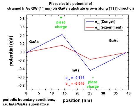
The piezoelectric charges are localized at the interfaces leading to a linear
potential.
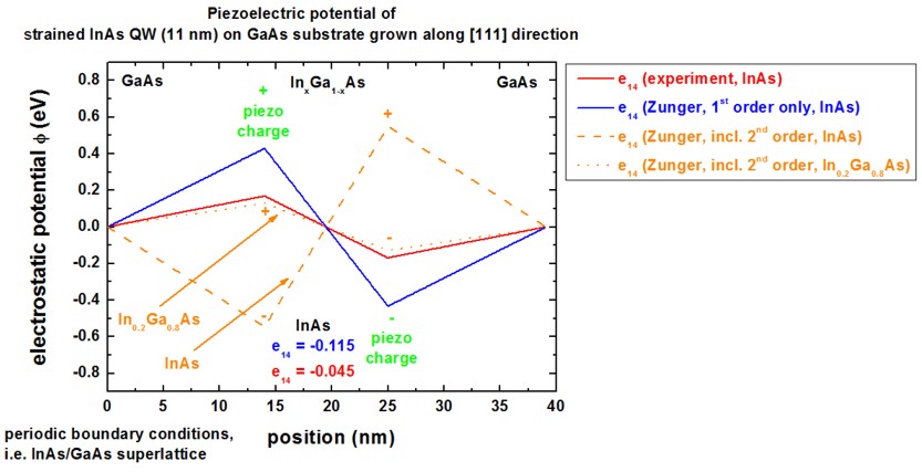
Piezoelectric potential including second-order terms for piezoelectric
polarization
 -> 1DInGaAsQW_onGaAs111_piezo_11nm_2ndOrder_nn3.in

    %Include2ndOrderPiezo =
yes


    %AlloyContent =
1.00   ! InAs
, alloy content In(x)Ga(1-x)As (DisplayUnit:)(ListOfValues:0.20,1.00)

    %AlloyContent =
0.20   ! In0.20Ga0.80As, alloy content
In(x)Ga(1-x)As (DisplayUnit:)(ListOfValues:0.20,1.00)
To include this effect, we have to switch on the 2nd order effect
for the piezoelectric polarization in
$numeric-control.
   piezo-second-order
=
no    ! (default)


=
yes   !
The following figure shows the same as above but this time including the
second-order terms B114, B124, B156 for the
piezoelectric polarization.
Note that the maximum value of our potential is at 0.55 eV whereas [Bester]
finds 0.85 eV for InAs.
Also included is the result for In0.2Ga0.8As (including
second-order terms, dotted line).
We found that at an Indium concentration of about x = ~0.60 the sign change
occurs ([Bester]: x = ~ 0.35).
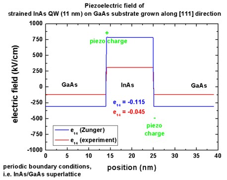
Piezoelectric field
    %Include2ndOrderPiezo =
no

    %AlloyContent =
1.00   ! InAs, alloy content
In(x)Ga(1-x)As (DisplayUnit:)

    %InAs_e14
= -0.045 ! 1st order piezoelectric coefficient e14
(InAs), experimental value (DisplayUnit:C/m^2) (ListOfValues:-0.045,-0.115)
The piezoelectric field is defined as F = - grad phipiezo.
Inside the InAs quantum well, the field has a positive value, which is
equivalent to a negative slope along the [111] direction for the piezoelectric
potential.
Note: [Bester] reports a negative value for the field although they have the
same slope.
The piezoelectric field is found to be ~ -1000 kV/cm for the case when
second-order terms are included whereas [Bester] finds ~ +1500 kV/cm.
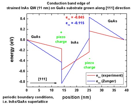
Conduction band edge
The following figure shows the resulting conduction band edge.
It is defined as Ec = Ec,0 - |e| phipiezo
= Ec,0 + Vpiezo
InGaAs quantum well between GaAs (realistic indium concentrations for
quantum wells)
-> 1DInGaAsQW_onGaAs111_piezo_nn3.in
Here, we have to modify the alloy content, and
the quantum well width.
    %AlloyContent =
0.21   ! In0.21Ga0.79As, alloy content
In(x)Ga(1-x)As (DisplayUnit:)(ListOfValues:0.17,0.21)

    %AlloyContent =
0.17   ! In0.17Ga0.83As, alloy content
In(x)Ga(1-x)As (DisplayUnit:)(ListOfValues:0.17,0.21)


    %QW_width     =
8.7   ! quantum well width (DisplayUnit:nm)(ListOfValues:8.7,10.0)

    %QW_width
= 10.0   ! quantum well width
(DisplayUnit:nm)(ListOfValues:8.7,10.0)


    %GaAs_e14     =
-0.160 ! 1st order piezoelectric coefficient e14 (GaAs),
experimental value S. Gironcoli et al., PRL 62(24), 2853 (1989) (DisplayUnit:C/m^2)

    %InAs_e14
= -0.045 ! 1st order piezoelectric coefficient e14
(InAs), experimental value (DisplayUnit:C/m^2)
Now we calculate three different InxGa1-xAs quantum
wells with different well widths and indium alloy contents and compare our
results to experimental data.
| quantum well material |
well width |
piezoelectric field (experiment) |
piezoelectric field (nextnano³) |
| In0.17Ga0.83As |
8.7 nm |
129 kV/cm +- 12 kV/cm
[Cho, 2001] |
196 kV/cm |
| In0.17Ga0.83As |
10 nm |
137 kV/cm +- 6 kV/cm [Sanchez, 2002] |
188 kV/cm |
| In0.21Ga0.79As |
10 nm |
121 kV/cm +- 5 kV/cm [Sanchez, 2002] |
223 kV/cm |
For these calculations, we used the experimental values for the piezoelectric
constants:
InAs: e14 = -0.045
C/m2
GaAs: e14 = -0.160 C/m2
The experimental trends
- "larger well width means larger field" and
- "more indium means less field"
cannot be reproduced.
We also note that our results for the piezoelectric field have the opposite
sign compared to the calculations of [Bester].
A different convention for the [111] direction (cation to anion vs. anion to
cation) could be a possible explanation for this.
|