nextnano3 - Tutorial
next generation 3D nano device simulator
1D Tutorial
Self-consistent 6-band k.p calculations of holes in strained Si/SiGe MOSFETs
Authors:
Stefan Birner
If you want to obtain the input files that are used within this tutorial, please
check if you can find them in the installation directory.
If you cannot find them, please submit a
Support Ticket.
-> 1DstrainedSi_SiGe_OberhuberPRB1998_step1_selfconsistent.in
-
self-consistent single-band Schrödinger equation
1DstrainedSi_SiGe_OberhuberPRB1998_step2_6x6kp_selfconsistent.in -
   1DstrainedSi_SiGe_OberhuberPRB1998_6x6kp_selfconsistent.in
-
Self-consistent 6-band k.p calculations of holes in strained Si/SiGe MOSFETs
This tutorial is based on the following paper:
[Oberhuber]
Subband structure and mobility of two-dimensional holes in strained
Si/SiGe MOSFET's
R. Oberhuber, G. Zandler, P. Vogl
Physical Review B 58, 9941 (1998)
Structure
We calculate the hole energy levels, wave function and density of the
following p-channel MOS structure:
Gate - SiO2
- strained Si - Si0.8Ge0.2
- Gate (applied voltage: VG = 1.6 V and 1.1 V)
- 5 nm SiO2
- 15 nm strained Si(001) with respect to Si1-xGex,
x=0.2, homogenously n-type doped 5 * 1016 cm-3
- 500 nm unstrained Si1-xGex buffer, x=0.2,
homogenously n-type doped 5 * 1016 cm-3
Both, Si and SiGe are n-type doped.
The method is 6-band k.p where we have to solve the Schödinger equation
(6-band k.p Hamiltonian) not only for k|| = 0
but also for a lot of k|| vectors, i.e. for k||
= (kx,ky) /= 0.
Our algorithm is the following:
-
1DstrainedSi_SiGe_OberhuberPRB1998_step1_selfconsistent.in
	-
self-consistent single-band Schrödinger equation
First, we solve the single-band Schrödinger equation and the Poisson
equation self-consistently.
This is useful because we want to obtain a reasonable start value for
the electrostatic potential.
	$simulation-flow-control

   ...

   raw-potential-in = no
	! STEP 1 only


	$quantum-model-holes
   ...

   model-name       =
	effective-mass ! STEP 1 only
(single-band)
-
1DstrainedSi_SiGe_OberhuberPRB1998_step2_6x6kp_selfconsistent.in -
self-consistent 6-band k.p
Schrödinger equation which reads in potential of single-band results as
initial guess
Then we read in the electrostatic potential calculated in 1) (which
serves as a start value for the electrostatic potential) and
solve the 6-band k.p Schrödinger equation and the Poisson equation
self-consistently (for both k|| = 0 and k||
/= 0).
	$simulation-flow-control

   ...

   raw-potential-in = yes
	! STEP 2
$quantum-model-holes
   ...

   model-name       =
	6x6kp
	 ! STEP 2
(6-band k.p)
1DstrainedSi_SiGe_OberhuberPRB1998_6x6kp_selfconsistent.in
	-
self-consistent 6-band k.p
Schrödinger equation
In principle, step 1 can be omitted but it helps to save some CPU time for step 2.
Note: If you want to avoid step 1, raw-potential-in
must be set to no. This is
then equivalent to this input file.
Note: "3" leads to the same results as "1" + "2"-
In agreement with [Oberhuber] (fur the purpose of this tutorial), we do not
allow the wave functions to penetrate into the SiO2 layer (i.e. we
assume infinite barriers at the SiO2/Si interface) although nextnano³
is general enough to also include the oxide into the quantum region if desired.
Material parameters
We use the same material parameters as quoted in the [Oberhuber] paper. The
only modification is the band offset.
We use a Ge-Si valence band offset, i.e. average of the three valence band edges
(Ev,av), of 0.58 eV (unstrained) and
for Si we take the following value for the absolute valence band deformation
potential:
 absolute-deformation-potential-vb = 2.05d0
! [eV]
This results in a band offset with respect to the topmost valence band edges:
heavy/light hole of Si0.8Ge0.2
(unstrained) - light hole strained Si = 0.046027 eV
Results
The following figure shows the valence band edge profile and the hole density
for two different gate voltages (VG = 1.6 V, VG = 1.1 V).
$poisson-boundary-conditions

   ...

applied-voltage = -1.6d0 ! VG
= 1.6 V Fig. 2(a) of [Oberhuber]
! applied-voltage = -1.1d0 !
Due to tensile strain, the topmost valence band in the strained Si layer is the
light hole band.
The heavy/light hole splitting for
strained Si on Si0.8Ge0.2 substrate: 79.7 meV ([Oberhuber]
80 meV)
In light gray, the squares of the topmost wave functions are indicated.
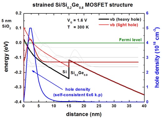
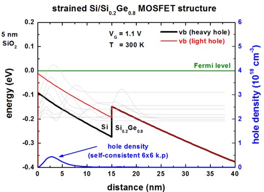
One can clearly see, that the inversion channel has a width of less than 10 nm.
At room temperature (300 K), in the Si layer only the 3-4 highest hole subbands
are significantly occupied (not shown).
The small density ("parasitic channel") in the SiGe layer is not due to these
3-4 states but due to other states.
In our calculations, the influence of the parasitic channel in the Si0.8Ge0.2
layer is negligible whereas [Oberhuber] found that only for high voltages (e.g.
VG = 1.6 V) it is negligible and for VG = 1.1 V almost 30
% of this density is contained in the parasitic channel.
The topmost subband (-31.3 meV for VG = 1.6 V,
-89.4 meV for VG = 1.1 V) has predominantly light-hole character whereas the
second, heavy-hole related subband lies
- 65.4 meV below the topmost subband (for VG = 1.6 V).
- 54.6 meV below the topmost subband (for VG = 1.1 V).
([Oberhuber] 55 meV)
The inversion layer sheet density (integrated over whole device) is found to
be:
- for VG = 1.6 V: ns = 1.85 * 1012
cm-2 ([Oberhuber], Fig. 2(a): ns = 1.2 *
1012 cm-2)
- for VG = 1.1 V: ns = 2.08 * 1011
cm-2 ([Oberhuber], Fig. 2(b): ns = 4
* 1011 cm-2)
Our results are in reasonable agreement with Fig. 2(a) and 2(b) of
[Oberhuber] considering the uncertainty in some assumptions (e.g. k||
space resolution, valence band offset, grid resolution).
Density of states (DOS)
The following figure shows the density of states (i.e. all eigenstates are
considered) for the two different gate voltages.
Note:
- At VG = 1.6 V, the valence band edge
maximum is approximately at Ev = 0.106 eV.
- At VG = 1.1 V, the valence band edge maximum is approximately
at Ev =
-0.010 eV.
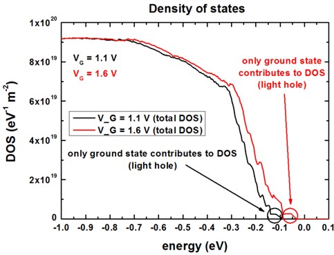
The total DOS output is contained in the following file: Schroedinger_kp/DOS_hl_sum_norm.dat
The following figure shows the density of states for the ground state (light
hole state) for the two different gate voltages.
(The DOS for the spin up state is very similar to the DOS of the spin down
state.)
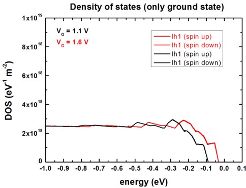
The DOS output for each eigenstate is contained in the following file:
Schroedinger_kp/DOS_hl_norm.dat
The DOS, as calculated within this 6-band k.p approach is used for
obtaining the self-consistent quantum mechanical hole density, thus taking into
account nonparabolicity rather than employing a parabolic energy dispersion E(kx,ky).
For more details on the density of states, see this tutorial:
Electron density of states (DOS) of a GaAs quantum well with infinite barriers
and
hole density of states (DOS) of a Si hole channel (triangular potential)
|